| Issue |
A&A
Volume 650, June 2021
Parker Solar Probe: Ushering a new frontier in space exploration
|
|
|---|---|---|
| Article Number | A27 | |
| Number of page(s) | 11 | |
| Section | Astronomical instrumentation | |
| DOI | https://doi.org/10.1051/0004-6361/202039754 | |
| Published online | 02 June 2021 | |
Thin silicon solid-state detectors for energetic particle measurements
Development, characterization, and application on NASA’s Parker Solar Probe mission
1
Jet Propulsion Laboratory, California Institute of Technology,
Pasadena,
CA
91109, USA
e-mail: This email address is being protected from spambots. You need JavaScript enabled to view it.
2
California Institute of Technology,
Pasadena,
CA
91125, USA
3
NASA Goddard Space Flight Center,
Greenbelt,
MD
20771, USA
4
Lawrence Berkeley National Laboratory,
Berkeley,
CA
94720, USA
5
Micron Semiconductor Ltd.,
Lancing,
Sussex,
BN15 8SJ, UK
6
Southwest Research Institute,
San Antonio,
TX
78228, USA
7
Department of Astrophysical Sciences, Princeton University,
Princeton,
NJ
08540, USA
8
Angold Consulting,
La Canada,
CA
91011, USA
9
University of New Hampshire,
Durham,
NH
03824, USA
Received:
24
October
2020
Accepted:
3
December
2020
Abstract
Context. Silicon solid-state detectors are commonly used for measuring the specific ionization, dE∕dx, in instruments designed for identifying energetic nuclei using the dE∕dx versus total energy technique in space and in the laboratory. The energy threshold and species resolution of the technique strongly depend on the thickness and thickness uniformity of these detectors.
Aims. Research has been carried out to develop processes for fabricating detectors that are thinner than 15 μm, that have a thickness uniformity better than 0.2 μm over cm2 areas, and that are rugged enough to survive the acoustic and vibration environments of a spacecraft launch.
Methods. Silicon-on-insulator wafers that have a device layer of the desired detector thickness supported by a thick handle layer were used as starting material. Standard processing techniques were used to fabricate detectors on the device layer, and the underlying handle-layer material was etched away leaving a thin, uniform detector surrounded by a thick, supporting frame.
Results. Detectors as thin as 12 μm were fabricated in two laboratories and successfully subjected to environmental and performance tests. Two detector designs were used in the High-energy Energetic Particles Instrument, which is part of the Integrated Science Investigation of the Sun instrument suite on NASA’s Parker Solar Probe spacecraft. These detectors have been performing well for more than two years in space.
Conclusions. Thin silicon detectors in d E∕dx versus total energy instruments enable the identification of nuclei with energies down to ~1 MeV nuc−1. This research suggests that detectors at least a factor of two thinner should be achievable using this fabrication technique.
Key words: instrumentation: detectors / Sun: particle emission / acceleration of particles / space vehicles: instruments
Present affiliation: Department of Astrophysical Sciences, Princeton University, Princeton, NJ 08540, USA.
© ESO 2021
1 Introduction
The measurement of energetic particle populations accelerated by magnetic reconnection in solar flares, by shocks driven by coronal mass ejections, or by shocks or compressions associated with solar wind stream interaction regions is an important tool for understanding these acceleration processes and the transport processes involved in distributing the accelerated particles in the heliosphere. Measurements over a wide range of energies, extending at least from several tens of keV nuc−1 to several tens of MeV nuc−1, are needed. This large range is typically covered using two different measurement techniques: time-of-flight (ToF) versus total energy (E) at low energies (e.g., Mason et al. 1998; Hill et al. 2017) and dE∕dx versus E (e.g., Stone et al. 1998a,b) at high energies. The transition between the two techniques commonly occurs in the vicinity of 1 MeV nuc−1, with some overlap of techniques when possible.
Extending the energy range covered by the dE∕dx versus E technique tolower energies is important because it will improve the energy overlap and, in some applications, allow the energy range of interest to be covered by a single instrument. The main factor limiting the low-energy extension of the d E∕dx versus E technique is the need for thin, mechanically robust dE∕dx detectors with a very uniform thickness. In this paper, we discuss the development of such detectors using silicon-on-insulator (SOI) wafers as the starting material. Section 2 discusses the required characteristics of such detectors. Section 3 describes the fabrication process. Section 4 presents data on the thickness characteristics that have been achieved. Section 5 discusses the measured detector performance, including DC electrical characteristics and the response to energetic particles. Section 6 discusses the results of some environmental tests that have been performed. Section 7 briefly discusses possibilities for further extending this technology.
2 Detector requirements
In the dE∕dx versus E technique, an energetic nucleus penetrates a thin detector (the “dE/dx” detector), depositing an energy ΔE, and comes to rest in a following thicker detector depositing its residual energy, E′. The threshold energy for obtaining these two-parameter measurements corresponds to a particle range equal to the sum of the silicon-equivalent thicknesses of the d E∕dx detector, the dead layer at the front of the E′ detector, any window in front of the dE∕dx detector, and the residual range required to reach the energy-detection threshold in the E′ detector. To penetrate 10 μm of silicon, an ion requires an energy of approximately 1 MeV nuc−1, with only a weak dependence on the atomic number, Z, of the ion because at these low energies the effective charges of higher-Z elements are reduced by the attachment of orbital electrons from the medium they are traversing. Thus, in order to measure energetic ions down to ~1 MeV nuc−1, the d E∕dx detector must have a thickness of L ≲ 10 μm. Several dE∕dx versus E instruments that have d E∕dx-detector thicknesses of ~15 μm have been used to study heavy-element composition in solar energetic particles (von Rosenvinge et al. 1978, 1995).
Applications requiring even thinner dE∕dx detectors are particularly challenging because of the difficulty of achieving sufficient thickness uniformity so that the “dx” involved in obtaining dE∕dx from the measured energy loss does not excessively degrade the charge and mass resolution. The Voyager Low Energy Charged Particle (LECP) experiment (Krimigis et al. 1977) used some small-area silicon detectors with thicknesses of ~5 and ~2 μm and was able to resolve major elements or element groups and investigate the origin and dynamics of energetic ion populations observed in the magnetospheres of Jupiter (Hamilton et al. 1981) and Saturn (Hamilton et al. 1983).
Further progress in extending the dE∕dx versus E technique tolower energies depends on the development of detectors that are not only thin but also have a high degree of thickness uniformity. In addition, achieving these characteristics in larger-area detectors is important for a variety of applications.
Stone et al. (1998a) discussed the contributions to mass resolution in dE∕dx versus E instruments and Mewaldt et al. (2008) applied such analysis to the case of elements and isotopes at a few MeV nuc−1 in the Low Energy Telescope (LET) instrument on NASA’s Solar TErrestrial RElations Observatory (STEREO) spacecraft. This instrument includes relatively thin (~22–30 μm) dE∕dx detectors. Uncorrectable variations in the thickness of dE∕dx detectors contribute a relative uncertainty in derived masses that is proportional to the relative uncertainty in the thickness of silicon penetrated, σM∕M ≃ kMσL∕L, where kM depends on the range-energy relation for the nuclei being measured. Similarly, these variations contribute to the relative charge resolution as σZ∕Z ≃ kZσL∕L. For the cases discussed here, kM ≃ 2 and kZ ≃ 0.4.
Thin silicon detectors of the type being discussed in this paper are operating in space in the High-energy Energetic Particles Instrument (EPI-Hi; McComas et al. 2016; Wiedenbeck et al. 2017), which is part of the Integrated Science Investigation of the Sun (IS⊙IS) energetic particle suite (McComas et al. 2016) on NASA’s Parker Solar Probe (PSP). This spacecraft was launched on 12 August 2018 on a mission designed to use multiple Venus gravity assists to penetrate deep into the solar corona and investigate the energetic particle environment close to the Sun (Fox et al. 2016).
The sensors in EPI-Hi include two “low-energy telescopes”, LET1 and LET2, that were designed to measure heavy ions down to energies ~1 MeV nuc−1. Figure 1 is a schematic cut-away illustration of LET1. This double-ended telescope has a pair of thin detectors, L0A (12 μm thickness) and L1A (25 μm thickness) at the front of the “A aperture” (top of Fig. 1) and a corresponding pair, L0B and L1B, at the front of the B aperture (bottom of the figure). In this paper we discuss the fabrication, characteristics, and performance of these detectors. The central stack of detectors in LET1 (L2A, L3A, L4A, L4B, L3B, and L2B) is involved in measuring particles that are sufficiently energetic to fully penetrate beyond both L0 and L1. The high-energy performance of the LET telescopes is discussed elsewhere (McComas et al. 2016; Wiedenbeck et al. 2017).
For measurements of He particles that penetrate L0 and stop in L1, achieving a mass resolution σM ≃ 0.25 amu for 4He requires σL ≃ 0.4 μm. This stringent requirement on thickness uniformity was one of the main drivers behind the thin-detector development. This same σL would lead to a charge resolution σZ ≃ 0.11 charge units (cu) for 8O and ≃0.35 cu for 26Fe.
Other key requirements for thin detectors are that they be rugged enough to survive the harsh acoustic and vibration environments associated with rocket launches and be capable of stable operation over a wide range of temperatures. In some applications, they must also be able to tolerate high doses of ionizing radiation, including that caused by the energetic nuclei they are being used to detect.
The requirements for thin, uniform detectors that have large areas but are still mechanically robustness are challenging. The following sections discuss the detectors that were developed to meet these requirements.
3 Detector fabrication
In order to produce thin, uniform silicon membranes, we use silicon-on-insulator (SOI) wafers purchased from commercial manufacturers as the starting material. A detailed discussion of processes used to make SOI wafers is beyond the scope of this paper, but they have been discussed in a number of reviews (e.g., Gosele & Tong 1998). In general, one starts with two relatively thick, conventional silicon wafers. A silicon dioxide layer of the desired thickness is grown on one or both wafers and the two wafers are assembled face-to-face with the silicon dioxide layer(s) between them. Applying pressure at elevated temperature leads to the van der Waals bonding of the surfaces. The result is a relatively strong mechanical bond formed without the use of an adhesive.
One wafer, called the “device layer”, is used for detector fabrication while the other wafer, called the “handle layer”, is used to provide mechanical support. Supported in this way, the device layer can be thinned by mechanical and/or chemical means to produce a layer that can be thin and, at the same time, very uniform. The thicknesses of the two silicon layers, as well as of the buried-oxide (BOX) layerbetween them, can be specified by the customer over fairly broad ranges. For the EPI-Hi detectors, thicknesses of (12 ± 0.3) μm (L0 detectors) or (25 ± 0.3) μm (L1 detectors), 0.65 μm, and 500 μm were specified for the device, BOX, and handle layers, respectively. We specified the 0.3 μm tolerance onthe device layer thicknesses on a “best-effort basis” because our specification was tighter than the best tolerance of 0.5 μm normally offered by the manufacturer1. The Lawrence Berkeley National Laboratory (LBNL) provided the float-zone refined silicon wafers that were used in producing the SOI’s device layers because this batch of wafers had previously been shown to yield good conventional detectors.
Figure 2 schematically illustrates a small section of an SOI wafer: (a) as received from the manufacturer and (b) after the processing steps that produce detectors’ pn junctions on the outward facing surface of the device layer and etching away the section of the handle layer and the BOX layer that underlie the detector. The handle layer retains its original thickness in regions not under the detectors.
The actual detector fabrication requires numerous steps involving masking, photolithography, ion implantation, annealing, surface passivation, evaporation of aluminum contacts, dicing, installation in mounts, and wire-bonding between pads on the detector chip and on the mount. These steps are routinely carried out during the fabrication of thicker detectors made using conventional silicon wafers and are discussed in various reviews (e.g., Wolf & Tauber 1998). The essential added step involved in making thin detectors from SOI wafers is the etching away of the handle-layermaterial. The processes involved in bulk etching of silicon crystals have also been reviewed (e.g., Kovacs et al. 1998).
Our detectors were fabricated from SOI for which single-crystal silicon wafers having a ⟨100⟩ orientation were used for both the device and handle layers. The etching was done in tetramethyl ammonium hydroxide (TMAH, (CH3)4NOH), which has been widely studied and used for bulk etching of silicon (e.g., Tabata et al. 1992). Silicon etches anisotropically in TMAH, with the etch proceeding most rapidly into ⟨100⟩ planes (parallel to the surfaces of our wafers) and most slowly into ⟨111⟩ planes. The etching produces broad, flat-surfaced recesses that terminate at their edges in sides that meet the surface at an angle of 54.74° ( ). The absolute silicon etching rate and the relative rates for different orientation planes depend on a variety of parameters such as temperature, concentration, amount of dissolved Si, and the presence of bubbles (which can locally interfere with the TMAH’s contact with the silicon). Producing silicon membranes of uniform thickness depends on the presence of the SOI wafer’s BOX layer. The etch rate for that layer’s silicon dioxide is much slower (by a factor of 100 or more) than for the silicon (e.g., Tabata et al. 1992). Thus the BOX layer provides an effective etch-stop. When the etching has reached the BOX layer, the SOI is removed from the etchant and inspected to make sure that there are no remaining hillocks of silicon on the BOX and that the BOX has not been penetrated. At that point, a short follow-up etch in hydrofluoric acid (HF) removes the exposed BOX material leaving a smooth silicon surface exposed through the opening in the handle layer.
During the etching, the SOI wafer is mounted so that the etchant cannot contact the outward-facing surface of the device layer, on which the detector structures, including the pn junctions, were previously fabricated.
Figure 3 shows a photograph of an EPI-Hi L0 detector viewed from the junction side (a) and from the ohmic side (b). The wide annular region of thin, inactive silicon in the L0 detector is needed to assure that all nuclei that have penetrated the 5-element central active regions of L1 and L2 (see Fig. 1) will have passed through the same overburden of silicon in L0, allowing the incident energies of these particles to be derived. The L1 detector looks very similar to L0, but lacks this thin, wide, inactive periphery and thus can have a smaller overall diameter (see McComas et al. 2016, Fig. 30c).
 |
Fig. 1 Schematic cut-away illustration of the LET1 telescope on PSP. Colors indicate different materials, as follows: orange–active silicon, yellow–inactive silicon, green–polyimide detector mounts, blue–Kapton windows, and brown and beige–aluminum telescope housing. The scale can be judged from the fact that the circle encompassing the five active segments of L0B has an area of 1 cm2. The figure was adapted from Wiedenbeck et al. (2017). |
 |
Fig. 2 Schematic illustration (not to scale) of a small section of a 100 or 150 mm diameter SOI wafer: (a) as received from the manufacturer and (b) after etching steps that remove the parts of the handle layer and buried oxide layers underlying the region that will form the thin detector. For the detectors made for the EPI-Hi instrument, the device, buried oxide, and handle-layer thicknesses were 12 (L0 detector) or 25 μm (L1 detector), 0.65, and 500 μm, respectively. |
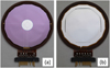 |
Fig. 3 Photograph of an L0 detector viewed from the junction surface (a) and from the ohmic surface (b). The junction surface is segmented into five active regions, consisting of a central bull’s eye surrounded by four quadrants, each with an active area of 0.2 cm2. This 5-segment structure is located at the center of a silicon membrane of 12 μm thickness, the remainder of which is not active. On the ohmic surface, the thin membrane is supported by an approximately octagonal, thick frame, the inner edge of which is visible in the photo. The shape of this edge is due to the different rates at which TMAH etches into different crystal planes. The ohmic surface, including the thin and the thick parts and the transition between them, is metallized with a single aluminum contact. |
4 Thickness characteristics
In order to understand the thickness characteristics of the completed detectors, the thin membrane portions of the detectors were mapped using an alpha-particle energy-loss technique, which is described in Appendix A. The left panel of Fig. 4 shows a contour plot of thicknesses over the full ~3.4 cm diameter of an L0 detector’s thin silicon membrane. Measured values are dominated by the silicon, but also include contributions from the aluminum metallization and an insulating SiO2 layer overlying it. The presence of the SiO2 only outside of the active area results in the difference of mean thickness between active and inactive areas and in the modification of the contours near the boundary. The right panel of the figure shows a histogram of thickness values for the entire measured area (unfilled) and restricted to the active area (filled). The extra material outside the active area increases the thickness of this region by up to ~1 μm silicon equivalent.
The thickness maps of the active region were obtained from measurements made using an array of points distributed approximately uniformly over its area. From those points, we have calculated a thickness mean and standard deviation. These are plotted as the circular points in Fig. 5. Open circles indicate detectors fabricated by Micron Semiconductor while filled points indicate the prototype detectors produced by the LBNL-Caltech collaboration. Data points for thin detectors of the two types developed for EPI-Hi are shown: L0 with a thickness of 12 μm and L1 with a thickness of 25 μm. In Fig. 5, the points corresponding to the two types are readily distinguishable because they cluster tightly near the two vertical dashed lines indicating the nominal silicon membrane thicknesses. This clustering provides a good indication of the capability of the SOI-based process for reliably yielding detectors of the desired thickness.
In contrast, Fig. 5 also shows, with × symbols, measurements of detectors that we previously flew in the Low Energy Telescope instrument (Mewaldt et al. 2008) on NASA’s STEREO mission. The STEREO LET detectors had active areas of 2 cm2 and target thicknesses specified to be in the range 18–22 μm. These detectors were fabricated from conventional silicon wafers (not SOI) that were lapped and polished to reduce their thickness to the desired range. As seen in the figure, nearly all of the detectors that were ultimately flown are thicker than the specified range, some significantly thicker. This is due to the fact that silicon wafers with thicknesses ≲ 20 μm are extremely fragile, and the manufacturing yield of such wafers was very low. Furthermore, they are very susceptible to breakage during detector manufacturing and testing.
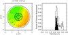 |
Fig. 4 Thickness measurements made over the thin area of an L0 detector. Left: contour map of thickness deviations from the value 12.27 μm at the central position. Right: histograms of thickness measurements in the central active area (filled) and over the full thin area (unfilled). The distribution of measurement locations across the membrane is shown in Fig. A.1. |
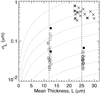 |
Fig. 5 Thickness, L, and rms thickness variation, σL, for various detectors, as follows: filled circles–prototype detectors made from SOI wafers for PSP EPI-Hiby the LBNL-Caltech collaboration; unfilled circles–detectors made from SOI wafers for PSP EPI-Hiby Micron Semiconductor; crosses–detectors made from conventional wafers for STEREO LET (Mewaldt et al. 2008) by Micron Semiconductor. The light, dotted lines indicate curves of constant σL ∕L with values (top to bottom) of 5, 2, 1, 0.5, 0.2, 0.1, and 0.05%. |
5 Detector performance
5.1 DC electrical characteristics
Measurements of detector capacitance (C) versus applied bias (V) were made in order to determine the full-depletion voltage (Vd) from CV curves. Typical values obtained were in the range 1.5 ± 0.3 V for both the L0 and the L1 detectors. The pulse heights obtained from alpha particles penetrating these detectors, as determined by looking at oscilloscope traces of output charge signals processed with a charge-sensitive amplifier and shaped with a time constant of a few μs, were indistinguishable for applied biases over the entire range studied (0–30 V).
Figure 6 shows plots of leakage current (I) versus applied bias (V) for typical L0 and L1 detectors at room temperature. For these measurements, the ohmic side of the detector was biased and the five main detector segments and also the annular area surrounding them were each individually held at a virtual ground by a precision op-amp used for processing the current signal. The plots show curves for each of the five segments, all of which have nearly the same current.
It is worth noting that if the outer annular region is allowed to float rather than being held at the same potential as the center segments, the currents measured on the four annular quadrant segments are much higher than the values plotted in the figure, but the current on the central bull’s eye segment is essentially unchanged. Apparently, the current from the outer region is diverted to the adjacent four segments with almost none of it reaching the bull’s eye segment.
Comparing the L0 and L1 IV curves in Fig. 6, it can be seen that the currents for these two detector types are essentially identical, in spite of the factor ~2 difference in the detector thicknesses. This suggests that the currents are dominated by surface effects, with negligible contribution from currents generated in the bulk volume of the silicon. This conclusion is supported by a comparison with currents observed in the L2 detectors (see Fig. 1), which have the same area and arrangement of five central segments as L0 and L1, but are 500 μm thick and made from conventional silicon wafers, not from SOI. For L2, the segment currents are ~400 nA, which is just 2× the corresponding L1 currents, not 20× as would be expected if the currents scaled as the active volume. This comparison provides only a qualitative indication because different silicon crystals were used for the two types of detectors.
5.2 Energetic particle response
The first few years of the PSP mission occurred at the minimum phase of the ~11-yr solar activity cycle and energetic particle activity was very low. However, at energies close to 1 MeV nuc−1, a number ofsmall events associated with particle acceleration near solar active regions or interplanetary stream interaction regions provided energetic H and He nuclei that were measured using the thin detectors (McComas et al. 2019; Cohen et al. 2020; Joyce et al. 2020; Leske et al. 2020; Wiedenbeck et al. 2020; Schwadron et al. 2020). The left panel of Fig. 7 shows examples of data accumulated from one of the apertures over a number of events. These measurements are compared with expected response tracks (black lines) derived using the Geant4 (GEometry ANd Tracking) simulation package (Allison et al. 2016). Such comparisons were used to fine-tune the average values of detector and dead-layer thicknesses used in the analysis.
The data in Fig. 7 were restricted to particles that triggered L0 and L1 detector segments that are vertically aligned (see L0B and L1B in Fig. 1), thereby selecting particles incident at relatively small angles, θ, from the telescope axis. This population of particles has a small spread in sec θ, which yields the best charge and mass resolution. The right panel of Fig. 7 shows the He mass histogram from the time period 20–21 Apr 2020 (day of year 110–111) when 3He-rich solar energetic particles were detected (Wiedenbeck et al. 2020). Fitting a Gaussian to the central part of the 4He peak (red curve) yields a standard deviation of 0.20 amu. We have found empirically that the smallest 3He/4He ratio that can reliably be detected at energies of a few MeV nuc−1 in d E∕dx versus E instrumentsusing silicon detectors is limited by tails on the low side of the 4He mass distribution2 to values of a few percent. Thus, further reduction of the standard deviation of the central Gaussian part of the peak would not help with the measurement of lower ratios. Non-aligned L0-L1 segment combinations are used in measuring angular distributions of heavy element fluxes, but are not suitable for resolving isotopes due to the range of sec θ values that they encompass.
Over the first two years of the PSP mission, EPI-Hi did not observe any events with intensities of Z > 2 nuclei high enough to adequately study the instrument response to these heavy ions. Thus, we have relied on measurements of accelerator beams to characterize the heavy element response of the thin detectors (Wiedenbeck et al. 2017). Figure 8 shows measurements made using a simple three-detector stack (left panel) read out with laboratory electronics at the LBNL 88-inch cyclotron. For this test, a “cocktail beam” containing a number of different ions with 16 MeV nuc−1 energy and a ratio of mass to ionic charge of ~2.9 was used. In addition, we did a test using a beam of low-energy 4He nuclei from a collimated alpha-particle source. These alphas are sufficiently energetic to penetrate the 12 μm detector and deposit their residual energy in the following 25 μm detector.
In order to populate response tracks using the mono-energetic particle populations from the accelerator or the radioactive source, we inserted an “energy spreader” in front of the detector stack. The spreader was made by stacking several layers of a thin, open-weave fabric mesh having fibers with circular cross sections. The wide range of thicknesses sampled by the particles spread out their energies. Since the resulting energy distribution was far from uniform, we sparsified the dataset to produce a more uniform distribution of energies deposited in the stopping detector. This sparsification procedure is responsible for some of the artifacts seen in Fig. 8. Others are due to particles entering or exiting the active area of detectors through the edges, to pulse pile-up in the electronics, and to channeling in the crystalline silicon.
In Fig. 8 we also show (dashed red lines) the locations of the response tracks expected from Geant4 simulations3. The most notable discrepancy between the measured and calculated tracks is apparent in the plot of E1 versus E2 (top right panel) where the lowest energy portions of some measured element tracks have lower E1 values than predicted from the simulation. It is well established that the mean ionic charge of heavy nuclei traversing material at low velocities is less than the nuclear charge due to the attachment of electrons from the stopping medium (e.g., Ahlen 1980). These effects, which are included among the physics processes accounted for in the Geant4 calculation, provide much better agreement than neglecting them entirely, but clearly further improvement should be possible. Additional discrepancies, which require further investigation, can be seen for some elements in the plot of E2 versus E3 (bottom right panel) at the highest E3 values. Once a sizable sample of heavy-ion events has been accumulated by the EPI-Hi instrument, we will be able to use those data to accurately determine the track locations. That calibration is important for onboard classification of detected heavy ions.
Wiedenbeck et al. (2017) show additional examples of the thin detector response to energetic nuclei at energies of a few MeV nuc−1 from radioactive sources and from a test at the Texas A&M University cyclotron. Since there is minimal variation of incidence angles (θ) among the particles in the accelerator beam, the charge resolution measured in those tests provides a lower limit on the resolution that can be expected in flight. There, the resolution will typically be dominated by the spread in secθ values. McComas et al. (2016) show some simulation results illustrating track separations expected when measuring heavy nuclei with isotropically distributed incidence angles.
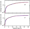 |
Fig. 6 Measurements of the leakage current for each of the five segments of two detectors: top–L0 detector (12 μm active thickness), bottom–L1 detector (25 μm active thickness). The curves for the individual segments, which are shown in different colors, are difficult to distinguish because the segments have very similar currents. |
6 Environmental tests
In order to assure that the thin detectors would survive the launch of the PSP spacecraft on a Delta IV-Heavy launch vehicle and perform as required in space, environmental tests were carried out at the individual detector level, in the assembled EPI-Hi instrument, and on the PSP spacecraft. Most of the tests were typical of those for many space launches. Here we briefly discuss a few aspects specific to the unique characteristics of this detector design and this mission.
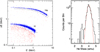 |
Fig. 7 Left: energy loss (ΔE) in the L0A detector versus residual energy (E′) deposited in L1A for energetic H and He nuclei collected by the EPI-Hi instrument during the early orbits of PSP. These data include particles incident through the A-end (generally sunward viewing end) of the LET1 telescope. The blue points indicate particles identified as H or He onboard; the red points indicate background events identified as not being consistent with any element. The region with a reduced density of points immediately below the H track is due to sampling of different regions of the plot with different efficiencies. Black lines show Geant4 calculations of the expected H, 3He, and 4He track locations. Right: He mass histogram from a two-day time period identified by Wiedenbeck et al. (2020) as having high values of 3He/4He (a few % or greater, as compared to ~0.04% in the solar wind). These He events were selected to have total energy greater than 4.8 MeV (E∕M > 1.2 MeV nuc−1 for 4He). Red line shows Gaussian fit to the central part of the 4He peak, which yields a mass resolution of 0.20 amu. |
6.1 Acoustics and vibration
The large ratio between the diameter of the thin area of crystalline silicon and its thickness, nearly 3000:1 for the L0 detectors, was regarded as a potential risk for mechanical damage in the acoustic and vibration environment of the launch. The concern over possible damage due to acoustics was heightened due to Caltech-JPL experience during the testing for the STEREO LET instrument (Mewaldt et al. 2008), which included silicon detectors with a thickness of ~25 μm and a diameter of ~1.6 cm (ratio 640:1). A significant fraction of those detectors broke during acoustic testing. Microscopic inspection of failed detectors showed thatcracks in the silicon usually started at locations along the edge where there had been chipping of the silicon, probably related to the dicing of the detectors out of the silicon wafer with a diamond saw. The STEREO LET detectors were fabricated from conventional silicon wafers that had been lapped and polished down to the desired ~25 μm thickness, not from SOI wafers. Flexing of the thin material in the region of the edge chipping increases the stress and causes a crack to propagate from the location of the chipping.
Unlike our STEREO LET experience, none of the PSP EPI-Hi detectors were damaged in acoustics or vibration testing. We suggest the difference is attributable to the fact that the thin device layer of the SOI-based detectors is supported over a width of at least several mm by the bonding to the thick handle wafer (see Fig. 3b), which greatly reduces the flexing that is possible near the edge.
Vibration could, in principle, also cause membrane flexing, but for these detectors the mass of thin silicon being accelerated is so small (<30 mg) that the force tending to flex the membrane is much less than in acoustics. No detector damage occurred as a result of the vibration tests.
6.2 Radiation
As an instrument designed to measure energetic nuclei down to ~1 MeV nuc−1, EPI-Hihas negligible radiation shielding to protect the thin silicon detectors, which reside at the front of the LET telescopes behind Kapton windows that are only a few μm thick (Wiedenbeck et al. 2017). Furthermore, the intensities of energetic particle events close to the Sun are expected to be higher than values commonly experienced near Earth, possibly increasing with decreasing heliocentric radius, r, as 1∕r2 or faster. The EPI-Hi instrument needs to continue to perform well even after exposure to this radiation environment (Lario & Decker 2011b,a) over the seven-year prime mission of PSP.
Total-dose tests were carried out at JPL using 60Co gamma rays up to a dose of 10 Mrad and a displacement damage test at the University of California Davis cyclotron was performed using a total fluence of 1013 /cm2 of 67.5 MeV protons. The significantly increased leakage currents measured following these radiation exposures were still at acceptable levels. The detector energy resolution, measured using an alpha-particle source, was not significantly degraded4.
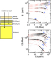 |
Fig. 8 Response of a simple detector telescope to heavy ions compared with a Geant4 simulation. Data were collected at the LBNL 88-inch cyclotron using a cocktail beam containing a variety of 16 MeV nuc−1 ions with M∕Q ≃ 2.9 including |


6.3 Dust impacts
A population of microscopic dust particles produced by multiple impacts of larger bodies pervades much of the inner heliosphere (Szalay et al. 2020, and references therein). At heliocentric distances that will be traversed by PSP, velocities of many such particles relative to the spacecraft will exceed several 100 km s−1. Impacts of these small, fast particles have the potential to penetrate the LET windows and impact the thin L0 detectors behind them. Therefore, tests were carried out at dust accelerators at the University of Colorado and at Heidelberg, Germany. The highest dust velocities and kinetic energies available from the accelerators were significantly less than could be encountered in flight, but did provide some useful insights into the effects that fast dust is likely to have. Dust particles were found to be able to penetrate the thin windows and produce pinholes comparable to the size of the dust particle, but the windows did not rupture. The LET design (Wiedenbeck et al. 2017) uses three windows spaced several mm apart (Fig. 1) to reduce the chance of light penetrating to the detectors5. Dust impacts on an L0 detector produced impact craters, but did not penetrate or rupture the detector. Impacts were found to cause significant and long-lasting increases in leakage current, but only the segment that was directly hit was affected. Successive impacts on the same segment had cumulative effects, producing an irregular stair-step increase of leakage current versus time.
Over the first six orbits of PSP, which reached heliocentric distances near 0.095 au, no leakage-current increases thought to be associated with dust impacts were observed. However, other PSP instruments have provided definitive evidence of dust impacts on the spacecraft, including one that punctured a very thin collimator foil on the IS⊙IS Low-energy Energetic Particles Instrument (EPI-Lo; McComas et al. 2016; Szalay et al. 2020).
6.4 Temperature
Parker SolarProbe was designed to allow instruments such as EPI-Hi to operate near room temperature (Fox et al. 2016) in spite of the intense heat input on the sunward-facing surface of the spacecraft. Thus, specifications called for the detectors to be tested between − 40 °C and + 40 °C for operation, similar to many near-Earth spacecraft, and between − 60 °C and + 60 °C for survival. These requirements were met without difficulty. The EPI-Hi thermal design passively cools the detector telescopes by radiation to space. Throughout the orbit, the detector temperatures have been stable around − 22 °C, which is conducive to low-noise operation.
7 Future prospects
The SOI-based approach for producing thin, uniform silicon detectors can be extended to yield even thinner devices. In one of our earliest efforts to make detectors from SOI wafers, Caltech thinned some SOI having device layers as thin as 5 μm, diced them into chips with thin areas ~1 cm2, and had Ametek-Ortec process those chips to make surface-barrier detectors. This detector type, which was commonly used prior to the widespread availability of ion-implanted detectors, employs a Schottky-barrier diode formed between the silicon and a metal evaporated on its surface. Detectors produced in this way detected alpha particles, but accelerator tests showed that under certain circumstances charge-multiplication effects (Tsyganov et al. 1996, and references therein) prevented reliable measurements of the energies deposited by heavier ions. These devices also had higher leakage currents than the ion-implanted detectors. The surface-barrier technology was rejected for further development, but these detectors did allow us to successfully demonstrate a process for SOI thinning.
More recently, the LBNL-Caltech collaboration made SOI-based, ion-implanted detectors with active areas as large as 4 cm2 and silicon membranes as thin as 5 μm. It was not possible to pursue testing of those devices because of the demands on Caltech personnel to develop the EPI-Hi instrument for PSP.
We anticipate that work in the near future will lead to SOI-based, ion-implanted detectors at least as thin as 5 μm that are suitable for spaceflight and laboratory applications.
Larger active areas are also of interest for future detector applications. Although the EPI-Hi L0 detector’s active area was only 1 cm2, that active region was located at the center of a 12 μm silicon membrane having an area of ~9 cm2 and the processing included fabrication of electrical traces that extend from the active area to the edge. Thus, it appears that it should be possible to produce detectors having at least this area and thickness. Since the capacitance per unit area of thin detectors is high (~900 pF cm−2 for a 12 μm detector), we would expect that large-area, thin detectors will be highly segmented. Thin silicon strip or pixel detectors seem like natural applications meriting further development.
Acknowledgements
We thank W. C. Tang for suggesting the use of SOI wafers as the basis for thin detector fabrication, B. Eyre for research on optimizing etching processes, J. Klemic (deceased) for developing the etching process used for thinning the detectors processed at LBNL, and B. D. Milliken for pioneering the technique used for thickness mapping. We thank S. Holland for useful discussions and S. M. Krimigis provided helpful comments about the thin silicon detectors used on Voyager. Important contributions to the success of the IS⊙IS EPI-Hiinstrument were made by numerous other scientists, engineers, and technicians. Particular thanks are due to G. Dirks, D. H. Do, J. J. Hanley, L. Hernandez, T. L. Johnson, S. Lopez, H. Miyasaka, G. Riggins, B. Rodriguez, K. Simms, and M. L. White. We gratefully acknowledge the test support provided by Michigan State University’s National Superconducting Cyclotron Laboratory, Texas A&M University’s Cyclotron Institute, and the Lawrence Berkeley National Laboratory’s 88-inch Cyclotron Laboratory. This work was supported, in part, by NASA’s Parker Solar Probe Mission, contract NNN06AA01C. Parker Solar Probe was designed, built, and is now operated by the Johns Hopkins Applied Physics Laboratory as part of NASA’s Living with a Star (LWS) program. Support from the LWS management and technical team has played a critical role in the success of the Parker Solar Probe mission. Earlier detector development work at JPL, Caltech, and LBNL was supported by several NASA grants. The IS⊙IS data and visualization tools are available to the community at https://spacephysics.princeton.edu/missions-instruments/isois; data are also available via the NASA Space Physics Data Facility (https://spdf.gsfc.nasa.gov/).
Appendix A Thickness measurements
Maps of the spatial dependence of thin-detector thicknesses were made to determine the mean thickness and thickness variation, as shown in Fig. 4. This appendix describes the non-contact method that was used to obtain calibrated measurements with a typical precision better than 0.1 μm. The general approach used was to allow a collimated beam of alpha particles from a radioactive source (244 Cm or 228Th) to penetrate the thin silicon membrane and then stop in a small silicon detector on the other side. The mean residual energy deposited in that detector is directly related to the thickness penetrated and can be calibrated by performing the corresponding measurement on samples of known thickness.
The left panel of Fig. A.1 is a schematic illustration of the setup. The alpha source and the silicon detector were mounted a few cm apart. A pair of sheet metal plates, each having one small hole (typically 2 mm diameter), were placed between the source and the detector, as shown. These parts were all held fixed relative to one another. The sample to be measured (detector or calibration foil) was inserted between the two collimator plates such that it could be moved in two dimensions perpendicular to the alpha-particle beam using a pair of computer-controlled translation stages. For the measurements, this assembly was installed in a vacuum system.
The sample being measured was successively moved to each of the points at which thickness measurements were desired (top right panel) and a spectrum of residual energies deposited in the detector was recorded. In the active region (red points), the point spacing was chosen to be comparable to the radius of the alpha particle beam. In the inactive outer region (blue points), a wider spacing was used to reduce the mapping time. Fits of Gaussians to the central portions of each of the residual-energy peaks yielded a setof means, standard deviations, and areas (numbers of counts) for the Gaussians. For many of the samples we studied, the variation of the mean over the area of the sample was smaller than the standard deviation. So, thousands of counts per point were typically used so that the location of the mean could be determined with the required precision.
In terms of g cm−2, a single sheet of household aluminum foil (not “heavy duty”) is equivalent to ~18 μm of silicon and in terms of the specific ionization, these two adjacent elements are very similar. So, for calibrating the measurements of the L0 (~12 μm) and L1 (~25 μm) detectors wechose to use 0, 1, and 2 layers of household aluminum foil. To obtain a precise value of the foil’s areal density, a full roll was unwound from its cardboard tube and weighed. Dividing the mass by the measured area of the foil yielded its mean areal density. Numerous samples were taken from various locations distributed over the foil to check the uniformity of the roll. We found the foil to be extremely uniform in thickness throughout the entire roll. Measurements of residual energies with each of the calibration samples in the alpha-particle beam were made for comparison with the silicon measurements.
After deriving the g cm−2 of aluminum required to produce the measured residual energies, we converted to equivalent g cm−2 of silicon using the ratio between the number of electrons per cm3 in aluminum and silicon. Finally, conversion from g cm−2 of silicon tothickness of silicon was done using the standard silicon density of 2.33 g cm−3. The small difference in electron binding energy between aluminum and silicon was neglected.
Rather than simply doing a linear interpolation between the calibration points, we used a modified interpolation procedure that takes advantage of the reasonably well known range-energy relation for alpha particles in silicon. This was motivated by the fact that silicon-equivalent thicknesses of 0, 1, and 2 layers of aluminum foil are fairly widely spaced, leading to inaccuracy in the linear interpolation. Our procedure depends on the alpha-particle range-energy relation,  , and its inverse function,
  .
.
We consider two samples with thicknesses Li and Lj. If alpha particles with a range Rα penetrate sample i (j) and deposit residual energy  (
( ) in the detector, the ratio of the residual energies, Γij, is related to Rα, Li and Lj by
 (A.1)
(A.1)
Letting samples i and j be the two calibration samples, Eq. (A.1) can be used to calculate Rα, which is the same for all of the measurements. Now, if the thickness Lk of another sample is to be derived by comparing its  with the calibration values
  and
and  , we just apply Eq. (A.1) to Γik using the same values of Li and Rα. Since this procedure does not depend on absolute values of the residual energies, but only on ratios among them, the calculation can be carried out using measured pulse heights without needing to know the gain of the electronics (providing that nonlinearities in these measurements are either negligible or corrected for).
Besides being insensitive to the electronic gain used for the residual energy measurements, the above procedure is also insensitive to the dead layer on the E′ detector and to any thin coating over the radioactive source. As long as these are the same for the calibration measurements as for measurements of the samples being studied, they do not play any role. Using the setup shown in the left panel of Fig. A.1, in which the source and detector are kept fixed relative to one another, these values remain the same for all measurements.
These measurements yield the physical thickness of the sample, not its active thickness. To date, we have treated the thin-detector dead layers as parameters that need to be adjusted to obtain the best agreement between the measured locations of ΔE–E′ tracks and locations calculated from a range–energy relation (see Fig. 7).
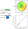 |
Fig. A.1 Left: schematic illustration of the setup used for mapping detector thicknesses. The locations of all parts were fixed relative to one another other than the sample being measured, which was translated in two dimensions perpendicular to the beam of α particles. Top right: locations at which measurements were made superimposed on the color contour map from Fig. 4. The red points are located within the active region of the detector; the blue points are located in the inactive peripheral region. The radius of the alpha beam at the detector was comparable to the distance between adjacent points in the active region. Bottom right: comparison of thicknesses derived from two separate runs mapping the same L0 detector. The error bars were derived from the statistical uncertainties in the mean positions of the Gaussians fitted to the residual energy distributions. Red (blue) indicates active (inactive) region points, as in the top right panel. |
References
- Ahlen, S. P. 1980, Rev. Mod. Phys., 52, 121 [Google Scholar]
- Allison, J., Amako, K., Apostolakis, J., et al. 2016, Nucl. Instrum. Methods Phys. Res. A, 835, 186 [Google Scholar]
- Cohen, C. M. S., Christian, E. R., Cummings, A. C., et al. 2020, ApJS, 246, 20 [Google Scholar]
- Fox, N. J., Velli, M. C., Bale, S. D., et al. 2016, Space Sci. Rev., 204, 7 [NASA ADS] [CrossRef] [Google Scholar]
- Gosele, U., & Tong, Q.-Y. 1998, Annu. Rev. Mater. Res., 28, 215 [Google Scholar]
- Hamilton, D. C., Gloeckler, G., Krimigis, S. M., & Lanzerotti, L. J. 1981, J. Geophys. Res., 86, 8301 [Google Scholar]
- Hamilton, D. C., Brown, D. C., Gloeckler, G., & Axford, W. I. 1983, J. Geophys. Res., 88, 8905 [Google Scholar]
- Hill, M. E., Mitchell, D. G., Andrews, G. B., et al. 2017, J. Geophys. Res. Space Phys., 122, 1513 [Google Scholar]
- Joyce, C. J., McComas, D. J., Christian, E. R., et al. 2020, ApJS, 246, 41 [Google Scholar]
- Kovacs, G. T., Maluf, N. I., & Petersen, K. E. 1998, Proc. IEEE, 86, 1536 [Google Scholar]
- Krimigis, S. M., Armstrong, T. P., Axford, W. I., et al. 1977, Space Sci. Rev., 21, 329 [Google Scholar]
- Lario, D., & Decker, R. B. 2011a, Space Weather, 9, S12002 [Google Scholar]
- Lario, D., & Decker, R. B. 2011b, Space Weather, 9, S11003 [Google Scholar]
- Leske, R. A., Christian, E. R., Cohen, C. M. S., et al. 2020, ApJS, 246, 35 [Google Scholar]
- Mason, G. M., Gold, R. E., Krimigis, S. M., et al. 1998, Space Sci. Rev., 86, 409 [Google Scholar]
- McComas, D. J., Alexander, N., Angold, N., et al. 2016, Space Sci. Rev., 204, 187 [Google Scholar]
- McComas, D. J., Christian, E. R., Cohen, C. M. S., et al. 2019, Nature, 576, 223 [Google Scholar]
- Mewaldt, R. A., Cohen, C. M. S., Cook, W. R., et al. 2008, Space Sci. Rev., 136, 285 [Google Scholar]
- Schwadron, N. A., Bale, S., Bonnell, J., et al. 2020, ApJS, 246, 33 [Google Scholar]
- Stone, E. C., Cohen, C. M. S., Cook, W. R., et al. 1998a, Space Sci. Rev., 86, 285 [Google Scholar]
- Stone, E. C., Cohen, C. M. S., Cook, W. R., et al. 1998b, Space Sci. Rev., 86, 357 [Google Scholar]
- Szalay, J. R., Pokorný, P., Bale, S. D., et al. 2020, ApJS, 246, 27 [Google Scholar]
- Tabata, O., Asahi, R., Hirofumi, F., Kenchi, S., & Sugiyama, S. 1992, Sens. Actuators, 34, 51 [Google Scholar]
- Tsyganov, Y., Kushniruk, W., & Polyakov, A. 1996, IEEE Transac. Nucl. Sci., 43, 2496 [Google Scholar]
- von Rosenvinge, T. T., McDonald, F. B., Trainor, J. H., Van Hollebeke, M. A. I., & Fisk, L. A. 1978, IEEE Transac. Geosci. Electron., 16, 208 [Google Scholar]
- von Rosenvinge, T. T., Barbier, L. M., Karsch, J., et al. 1995, Space Sci. Rev., 71, 155 [Google Scholar]
- Wiedenbeck, M. E., Angold, N. G., Birdwell, B., et al. 2017, Int. Cosmic Ray Conf., 301, 16 [Google Scholar]
- Wiedenbeck, M. E., Bučík, R., Mason, G. M., et al. 2020, ApJS, 246, 42 [Google Scholar]
- Wolf, S., & Tauber, R. N. 1998, Silicon Processing for the VLSI Era, Process Technology (Sunset Beach, CA: Lattic Press), 1 [Google Scholar]
Ultrasil Corp., Hayward, CA USA.
Low-side tails are primarily due to channeling effects in the crystalline silicon.
The Geant4 emstandard_opt3 physics option was used.
In one prototype detector design, the contact to the ohmic surface was made through the bulk of the inactive silicon near the edge of the device layer. The displacement damage test increased the resistivity of this n-type silicon and made the RC time constant due to the combination of this resistive contact and the large detector capacitance comparable to the few μs of the pulse-shaping circuit and reduced the measured pulse height. However, paralleling this contact with a conventional wire-bond contact directly to the ohmic surface restored the pre-exposure pulse heights. On all of the flight detectors, wire bonds to the ohmic surface were used.
Near the Sun, EPI-Hi is always in the shadow of the PSP heat shield, but it is still possible for some scattered light from the solar corona to reach the instrument.
All Figures
|
Fig. 1 Schematic cut-away illustration of the LET1 telescope on PSP. Colors indicate different materials, as follows: orange–active silicon, yellow–inactive silicon, green–polyimide detector mounts, blue–Kapton windows, and brown and beige–aluminum telescope housing. The scale can be judged from the fact that the circle encompassing the five active segments of L0B has an area of 1 cm2. The figure was adapted from Wiedenbeck et al. (2017). |
| In the text | |
|
Fig. 2 Schematic illustration (not to scale) of a small section of a 100 or 150 mm diameter SOI wafer: (a) as received from the manufacturer and (b) after etching steps that remove the parts of the handle layer and buried oxide layers underlying the region that will form the thin detector. For the detectors made for the EPI-Hi instrument, the device, buried oxide, and handle-layer thicknesses were 12 (L0 detector) or 25 μm (L1 detector), 0.65, and 500 μm, respectively. |
| In the text | |
|
Fig. 3 Photograph of an L0 detector viewed from the junction surface (a) and from the ohmic surface (b). The junction surface is segmented into five active regions, consisting of a central bull’s eye surrounded by four quadrants, each with an active area of 0.2 cm2. This 5-segment structure is located at the center of a silicon membrane of 12 μm thickness, the remainder of which is not active. On the ohmic surface, the thin membrane is supported by an approximately octagonal, thick frame, the inner edge of which is visible in the photo. The shape of this edge is due to the different rates at which TMAH etches into different crystal planes. The ohmic surface, including the thin and the thick parts and the transition between them, is metallized with a single aluminum contact. |
| In the text | |
|
Fig. 4 Thickness measurements made over the thin area of an L0 detector. Left: contour map of thickness deviations from the value 12.27 μm at the central position. Right: histograms of thickness measurements in the central active area (filled) and over the full thin area (unfilled). The distribution of measurement locations across the membrane is shown in Fig. A.1. |
| In the text | |
|
Fig. 5 Thickness, L, and rms thickness variation, σL, for various detectors, as follows: filled circles–prototype detectors made from SOI wafers for PSP EPI-Hiby the LBNL-Caltech collaboration; unfilled circles–detectors made from SOI wafers for PSP EPI-Hiby Micron Semiconductor; crosses–detectors made from conventional wafers for STEREO LET (Mewaldt et al. 2008) by Micron Semiconductor. The light, dotted lines indicate curves of constant σL ∕L with values (top to bottom) of 5, 2, 1, 0.5, 0.2, 0.1, and 0.05%. |
| In the text | |
|
Fig. 6 Measurements of the leakage current for each of the five segments of two detectors: top–L0 detector (12 μm active thickness), bottom–L1 detector (25 μm active thickness). The curves for the individual segments, which are shown in different colors, are difficult to distinguish because the segments have very similar currents. |
| In the text | |
|
Fig. 7 Left: energy loss (ΔE) in the L0A detector versus residual energy (E′) deposited in L1A for energetic H and He nuclei collected by the EPI-Hi instrument during the early orbits of PSP. These data include particles incident through the A-end (generally sunward viewing end) of the LET1 telescope. The blue points indicate particles identified as H or He onboard; the red points indicate background events identified as not being consistent with any element. The region with a reduced density of points immediately below the H track is due to sampling of different regions of the plot with different efficiencies. Black lines show Geant4 calculations of the expected H, 3He, and 4He track locations. Right: He mass histogram from a two-day time period identified by Wiedenbeck et al. (2020) as having high values of 3He/4He (a few % or greater, as compared to ~0.04% in the solar wind). These He events were selected to have total energy greater than 4.8 MeV (E∕M > 1.2 MeV nuc−1 for 4He). Red line shows Gaussian fit to the central part of the 4He peak, which yields a mass resolution of 0.20 amu. |
| In the text | |
|
Fig. 8 Response of a simple detector telescope to heavy ions compared with a Geant4 simulation. Data were collected at the LBNL 88-inch cyclotron using a cocktail beam containing a variety of 16 MeV nuc−1 ions with M∕Q ≃ 2.9 including |
| In the text | |
|
Fig. A.1 Left: schematic illustration of the setup used for mapping detector thicknesses. The locations of all parts were fixed relative to one another other than the sample being measured, which was translated in two dimensions perpendicular to the beam of α particles. Top right: locations at which measurements were made superimposed on the color contour map from Fig. 4. The red points are located within the active region of the detector; the blue points are located in the inactive peripheral region. The radius of the alpha beam at the detector was comparable to the distance between adjacent points in the active region. Bottom right: comparison of thicknesses derived from two separate runs mapping the same L0 detector. The error bars were derived from the statistical uncertainties in the mean positions of the Gaussians fitted to the residual energy distributions. Red (blue) indicates active (inactive) region points, as in the top right panel. |
| In the text | |
Current usage metrics show cumulative count of Article Views (full-text article views including HTML views, PDF and ePub downloads, according to the available data) and Abstracts Views on Vision4Press platform.
Data correspond to usage on the plateform after 2015. The current usage metrics is available 48-96 hours after online publication and is updated daily on week days.
Initial download of the metrics may take a while.