Fig. 2
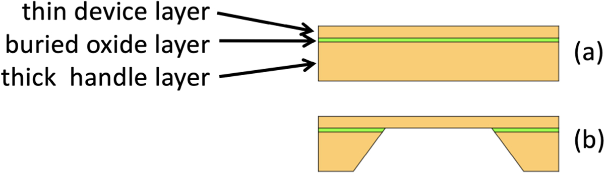
Schematic illustration (not to scale) of a small section of a 100 or 150 mm diameter SOI wafer: (a) as received from the manufacturer and (b) after etching steps that remove the parts of the handle layer and buried oxide layers underlying the region that will form the thin detector. For the detectors made for the EPI-Hi instrument, the device, buried oxide, and handle-layer thicknesses were 12 (L0 detector) or 25 μm (L1 detector), 0.65, and 500 μm, respectively.
Current usage metrics show cumulative count of Article Views (full-text article views including HTML views, PDF and ePub downloads, according to the available data) and Abstracts Views on Vision4Press platform.
Data correspond to usage on the plateform after 2015. The current usage metrics is available 48-96 hours after online publication and is updated daily on week days.
Initial download of the metrics may take a while.