| Issue |
A&A
Volume 580, August 2015
|
|
|---|---|---|
| Article Number | A15 | |
| Number of page(s) | 6 | |
| Section | Astronomical instrumentation | |
| DOI | https://doi.org/10.1051/0004-6361/201526206 | |
| Published online | 21 July 2015 | |
Bi-layer kinetic inductance detectors for space observations between 80–120 GHz
1 Laboratoire de Physique Subatomique et de Cosmologie, LPSC, Université Grenoble-Alpes, CNRS/IN2P3, 53 rue des Martyrs, 38026 Grenoble Cedex, France
e-mail: This email address is being protected from spambots. You need JavaScript enabled to view it.
2 Institut Néel 38042, CNRS, Université Joseph Fourier Grenoble I 38042, 25 rue des Martyrs, 38026 Grenoble, France
3 Centre de Sciences Nucléaires et de Sciences de la Matière (CSNSM), CNRS/IN2P3, Bât. 104–108, 91405 Orsay, France
4 Institut de Planétologie et d’Astrophysique de Grenoble (IPAG), CNRS and Université de Grenoble, 38026 Grenoble, France
5 LNGS – Laboratori Nazionali del Gran Sasso, via G. Acitelli 22, 67100 Assergi L’ Aquila, Italy
Received: 28 March 2015
Accepted: 28 May 2015
Abstract
We have developed lumped element kinetic inductance detectors (LEKIDs) that are sensitive in the frequency band from 80 to 120 GHz. In this work, we take advantage of the so-called proximity effect to reduce the superconducting gap of aluminium (Al), otherwise strongly suppressing the LEKID response for frequencies smaller than 100 GHz. We designed, produced, and optically tested various fully multiplexed arrays based on multi-layer combinations of Al and titanium (Ti). Their sensitivities were measured using a dedicated closed-circle 100 mK dilution cryostat and a sky simulator, which allowed us to reproduce realistic observation conditions. The spectral response was characterised with a Martin-Puplett interferometer up to THz frequencies and had a resolution of 3 GHz. We demonstrate that Ti–Al LEKID can reach an optical sensitivity of about 1.4 × 10⁻¹⁷ W/Hz0.5 (best pixel), or 2.2 × 10⁻¹⁷ W/Hz0.5 when averaged over the whole array. The optical background was set to roughly 0.4 pW per pixel, which is typical for future space observatories in this particular band. The performance is close to a sensitivity of twice the CMB photon noise limit at 100 GHz, which drove the design of the Planck HFI instrument. This figure remains the baseline for the next generation of millimetre-wave space satellites.
Key words: instrumentation: detectors / space vehicles: instruments / instrumentation: photometers / cosmic background radiation
© ESO, 2015
1. Introduction
The study of the cosmic microwave background (CMB) temperature and polarisation anisotropies has become a powerful tool for cosmology thanks in particular to the spatial observations of the COBE (Kogut et al. 1996), the WMAP (Bennett et al. 2013) and Planck satellites (Planck Collaboration I 2014). The Planck mission has provided detailed temperature and polarisation CMB maps (Planck Collaboration XVI 2014), but it was not conceived as the ultimate instrument for CMB polarisation measurements, and it will most probably only marginally measure primordial CMB polarisation B-modes. The latter are only sourced by tensor perturbations in the early Universe and are predicted by inflation (Hu & White 1997). To improve this situation, new CMB space missions such as CORE+1, PIXIE (Kogut et al. 2011), LiteBIRD (Matsumura et al. 2014), are discussed.
In this context, space observations at about and slightly below 100 GHz have proved to be fundamental for CMB science, as they lie in the frequency range for which Galactic foreground contamination is minimal both in intensity and polarisation (Plank Collaboration Int. XXIX 2014; Fauvet et al. 2012, 2011). The Planck mission2 was equipped with 11 HEMT (Low Frequency Instrument, LFI, Mennella et al. 2011) and 52 high-impedance bolometers (High Frequency Instrument, HFI, Planck HFI Core Team 2011) observing from 30 GHz to 1 THz. Of these, eight polarised sensitive bolometers (PSB) with a bandpass centred at 100 GHz (Δν/ν = 0.33) were used to survey the sky in temperature and polarisation at an angular resolution of about 10 arcmin. This provided HFI with a powerful tool to detect and precisely measure the CMB E-modes, but not the primordial B-modes, which are expected to be much fainter (Planck Collaboration XVI 2014). To meet the challenge of measuring CMB polarisation B-modes, it is necessary to improve the instrumental sensitivity by at least one order of magnitude with respect to Planck. In terms of noise-equivalent power, this corresponds to expanding from 10-17 WHz−1/2 to 10-18 WHz−1/2. This can be achieved by increasing the focal plane coverage by using thousands of background-limited instrument performance (BLIP) contiguous pixels.
Kinetic inductance detectors (KID; Day et al. 2003) have now reached a maturity that is adequate for space instruments. The first demonstration of this maturity was achieved by ground-based experiments and in particular by the New IRAM KID Array (NIKA) instrument. NIKA is a dual-band camera operating with frequency-multiplexed arrays of lumped element kinetic inductance detectors (LEKIDs) that are based on aluminium (Al) films and are cooled at 100 mK (Monfardini et al. 2011). The NIKA instrument exhibits very high sensitivity in the 120–300 GHz band range (Catalano et al. 2014).
The frequency range below 120 GHz is not accessible using the NIKA Al films because of the superconducting gap cut-off. Therefore we need to adopt lower superconducting gap films. Several authors have investigated titanium nitride (TiN) as an alternative to Al KID (Swenson et al. 2013; Leduc et al. 2010; Bueno et al. 2014) in the past years. In parallel, we have studied a large number of possible alternative solutions. These included investigating Nb(x)Si(1−x) as a promising alloy to be used at these frequencies (Calvo et al. 2014). Here we use a different approach: we start from Al, which has given the best performances up to now, and lower its gap using the superconducting proximity effect with Ti.
This paper is structured as follows. In Sect. 2, we give the main ingredients of the bi-layer LEKID design and describe its fabrication process; details on the noise and responsivity of a LEKID array are also presented. In Sect. 3, we describe the experimental setup. Section 4 presents the measurements and the results we obtained. We draw conclusions in Sect. 5.
2. LEKID detectors
Here we review the basic ingredients that are necessary to discuss the design and to evaluate the performances of the Ti–Al bilayer LEKID. The general KID theory was first established by Day et al. (2003). For a complete review, we refer to Zmuidzinas (2012) and Doyle (2008). LEKID is a resonator that is fabricated from superconducting elements in which absorbed photons can change the Cooper-pair density, producing a change in both resonant frequency and the quality factor of the resonator. LEKID arrays are based on series of LC resonators of different eigenfrequencies, coupled to a single 50 Ω feed-line. The term lumped element describes the fact that the resonator is smaller than the wavelength at the resonance frequency. In addition, lumped element devices directly act as the absorber of GHz–THz photons, which greatly simplifies the design and array fabrication. Furthermore, one needs to match their sheet impedance to the incoming photons, which implies using either very thin or quite resistive layers. In that respect, Ti is preferable to noble metals such as Au, Ag, or Cu for tuning the superconducting gap of Al.
2.1. Tuning the gap cut-off with proximity effect
The lowest photon energy that can be absorbed in a superconductor below the critical temperature is equal to twice the superconducting gap Δ0. For standard3 superconductors  (1)where kB is the Boltzmann constant and Tc is the critical temperature of the transition to the superconducting state.
Adjusting Tc is therefore important for tuning the absorption of photons to the suitable frequency. The possibility of tuning the transition temperature of a superconductor through the proximity effect with a normal metal (or another superconductor) is a well-known property of superconductivity. It has been successfully exploited in transition-edge sensors to operate bolometers at a lower temperature and hence lower their specific heat (Irwin & Hilton 2005; Nagel et al. 1994). Here we also exploit the proximity effect, but in this case, to lower the energy threshold of detectable photons.
A comprehensive calculation of the Tc of bi-layers is given in Martinis et al. (2000). More generally, all relevant properties (in particular the density of states) can be derived in the framework of the Usadel theory (Usadel 1970), which describes inhomogeneous superconductors. Two coupled non-linear differential equations need to be solved (most often numerically), which describe the diffusion of electronic excitations (single and paired) in an inhomogeneous pair potential that is provided by boundary conditions at the interfaces. Here we consider that the contact between the two layers is perfect and that the average transmission is unity, which provides the strongest proximity effect. Furthermore, the superconducting coherence length is assumed to exceed the thickness of the film, and thereby superconducting properties are homogeneous over the thickness.
In this case, an approximate analytical solution can be derived following Cooper’s intuitive approach (Cooper 1961), which considers the bi-layer as a superconductor with an effective pairing potential NVeff. As electrons spend a fraction of time N1d1/ (N1d1 + N2d2) in layer 1, this effective potential writes
 where Nx is the electron density, Vx the electron-phonon coupling and dx the thickness of layer x. This effective potential is then used to calculate Tc in the standard superconductor gap equation kBTc ≃ 1.13ħωD·e(− 1 /NVeff), where ωD is the Debye frequency. This approach is only valid when the vibration properties of the two layers are identical, which is roughly the case for Ti and Al. From this simple formula, the general trend of which is confirmed by more thorough calculations, the great convenience of bi-layers is clear since their critical temperature can be finely tuned by changing the relative thickness of the components. For the Ti 10 nm/Al 25 nm bi-layers fabricated in this work, the expected Tc is between 850 mK and 920 mK. This uncertainty comes from the fact that we need to take into account an increase of the Tc of Al at 25 nm compared to the bulk value (the discussion of which is not the purpose of the present work). In a standard superconductor, this yields a frequency threshold for photon absorption between 62 GHz and 68 GHz. A last argument for choosing Ti instead of noble metals comes from its weak solubility in Al, which improves predictability, reproducibility, and robustness of the devices to ageing.
2.2. Optical responsivity
The optical responsivity for a LEKID represents the relation between a variation of the incident optical power and the shift in the resonant frequency of the detector ( ). This measured variation is determined by the change in internal inductance of the film with a change in Cooper-pair density induced by incoming photons.
For the LEKID, all the properties directly related to the calculation of the responsivity affect each other, so that it is not possible to derive a general single analytical formula. For a detailed study of the parameters that determine the responsivity of a LEKID we refer to Doyle et al. (2007, 2008).
2.3. Noise
The detector noise-equivalent power (NEP), in W/ , is defined as the optical signal that is equal to the noise in a 1 Hz amplifier bandwidth at the output. This quantity takes into account the response and the spectral noise density Sn(f) of the detector (in Hz/
 ). All the uncorrelated sources of noise add quadratically:
  (2)The detectors noise NEPdet may come from random variations of the effective dielectric constant or fluctuations of the Cooper-pair density that are due to generation-recombination noise4. NEPel is the noise associated with the full readout electronics chain (cold and warm). Finally, NEPphot represents the source of noise related to the photon noise that comes from the fluctuations of the incident radiation that are due to the Bose-Einstein distribution of the photon emission. This noise corresponds to the ultimate limitation in sensitivity of any instrument because it does not depend on detector performance and readout electronics. Considering a satellite orbiting the second Lagrange point of the Earth-Sun system, the in-space photon noise level per pixel at 100 GHz with a bandwidth Δν/ν = 0.3 is equal to about 0.5 × 10⁻¹⁷ W/.
As a guideline, for future-generation millimetre satellites as well as for Planck HFI, the goal NEP per pixel has been defined as  (3)When this condition is satisfied, we refer to photon-noise dominated detectors. We keep this definition as a reference to compare the results obtained in this paper.
2.4. LEKID module design, fabrication, and assembly
For the first-generation Ti–Al arrays, we adopted single-polarisation LEKID designed originally for Al films (Fig. 1). The first prototype of Ti–Al arrays comprises 25 pixels. The LEKID holder allows back-illumination through the silicon substrate. This method works better than directly illuminating the LEKID because high-permittivity silicon substrate has a far lower impedance than that of free space. In front of the LEKID, a superconducting lid acts as a λ/ 4 back-short, optimising the absorption in the frequency band of interest. A schematic of this arrangement is shown in Fig. 1.
Each pixel is a resonator composed of a meander inductor and an interdigitated capacitor. The 4 μm wide lines of the meander are the smallest features in the current design. The 25 pixels are inductively coupled to a coplanar wave guide (CPW) 50Ω line. We added wire-bonds to make air-bridges across the CPW at a distance of few millimetres between each other. The fabrication starts with a high-resistivity (>6000 Ω·cm), 525 μm thick silicon [111] mono-crystalline wafer. The native silicon oxide is etched with an HF:H2O 5% solution, then rinsed in H2O. This step passivates the Si bonds on the surface, replacing O with H. The wafer is then put under vacuum within the next 30 min to prevent re-oxidation. The bi-layer is coated in situ by e-beam evaporation under a ≈3e−8 mb vacuum. A 10 nm thick titanium film is first deposited, followed directly by a 25 nm thick aluminium film. This ensures that there is no oxidation layer at the interface between titanium and aluminium and ensures the highest proximity effect between the two layers. The next step is a standard photo-lithographic process, with a positive resin (AZ1512Hs). The etching is made in two phases, first with an Al-etch dip, then with a diluted 0.1% HF solution to etch Ti. After dicing, the array is mounted on a dedicated holder, and the CPW is wire-bonded to the launcher with an Al-Si wire.
2.5. Readout system
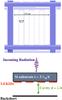 |
Fig. 1 Single Ti–Al bi-layer LEKID resonator design (top). The resonator is composed of a long inductive meander line and a capacitive element that is also used for tuning the resonant frequency. The effective sheet impedance of the meander line (seen by GHz–THz photons) is adjusted by the geometrical filling factor for a given the film resistivity. To optimise 100 GHz photon absorption, the pixels are back-illuminated through the silicon substrate. In addition, we use a back-short cavity situated at an optimised distance of 750 μm from the pixels (bottom). |
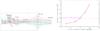 |
Fig. 2 Left: ray-tracing snapshot of the cold optics inside the cryostat. Right: optical background estimation as a function of 100 mK cold stop aperture diameter (red line). We compare this result to the optical background measured in the HFI 100 GHz channel (violet dashed line). |
We used a vector network analyser (VNA) to measure the LEKID responsivity and the NIKEL electronics (described in Bourrion et al. 2012) to measure the spectral response and characterise the noise. The NIKEL electronics has been successfully used during several NIKA observing campaigns (Catalano et al. 2014; Adam et al. 2014). We briefly describe the readout concept. We generated a frequency comb that is up converted by mixing with a local oscillator carrier at the appropriate frequency that corresponds to the best-estimate resonant frequency for each pixel. On the output line, the signal is boosted by a cryogenic low-noise amplifier and then is down-converted to the base band and acquired by an analogue-to-digital converter (ADC). Finally, the useful signal is computed on-board with an FPGA: each output tone is compared to a copy of the input tones that is kept as a reference, so that for each pixel we extract the in-phase (I) and quadrature (Q) components of the signal.
The knowledge of the I and Q components alone does not give full access to the change in resonance frequency that is due to an incoming optical signal. To do so, we also modulated the frequency on the local oscillator (by few kHz) synchronously to the FPGA to recover the differential values dI and dQ in addition to the I and Q components. More details of this technique are presented in Calvo et al. (2013).
3. Optical background control
To characterise the optical response of the Ti–Al array, we used a testing device called Sky Simulator (hereafter SS). It was originally built to mimic the typical ground optical background for the NIKA instrument at the IRAM 30 m telescope at Pico Veleta (Monfardini et al. 2011). The working principle is based on cooling down a black disk of 25 cm diameter by using a single-stage pulse-tube refrigerator. The SS temperature can be controlled to be between 50 K and 300 K. This allows us to efficiently estimate the optical detector response and the NEP. The spectral response of the detectors is derived from a classic Martin-Puplett Interferometer (hereafter MPI) based on a blackbody source modulated between 300 K and 77 K and fully polarised by a wire-grid.
The optical coupling between the SS (or the MPI) and the detectors is ensured by cold refractive optics. The optical system consists of a 300 K window lens, a field stop, and a lens at the 4 K stage. A 60 mm aperture stop and a lens are placed at the 100 mK stage in front of the back-illuminated LEKID arrays. Finally, to acquire data simultaneously with two independent RF channels, a wire-grid polariser acts as beam splitter for the two arrays. The left panel of Fig. 2 shows a 2D layer snapshot from the ray-tracing simulation that was used to optimise the optical system.
The pixel throughput5 is derived from the sky-simulator diameter, the fraction of un-vignetted pupil defined by the cold field stop, and the receiver pixel size with respect to the diffraction pattern. We obtain
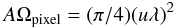 where u is the pixel angular size in units of Fλ (λ = wavelength and F= f-number or relative aperture), which is equal to 0.75. The spectral band is defined by a series of low-pass metal mesh filters that are placed at different cryogenic stages to minimise the thermal loading of the detectors. A last 3.7 cm-1 low-pass filter is mounted in front of the LEKID array at 100 mK. The final bandpass is determined by this filter at high frequencies and by the superconducting gap cut-off at low frequencies.
We performed an optical simulation of the system accounting for the absorption, reflection and emission of the polyethylene lenses and the diffracted beam that is due to the cold aperture stop at 100 mK to estimate the optical background on the focal plane. The results of this simulation were validated by comparing the optical background on NIKA Al arrays for laboratory tests to the one measured at the 30 m IRAM telescope. We estimate the level of uncertainties to be about 50%. To re-scale the total optical background on each pixel to the typical in-flight optical background at 100 GHz, we reduced the cold aperture from 60 to 20 mm and obtained an incoming optical power of about 0.4 pW (see Fig. 2).
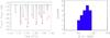 |
Fig. 3 Left: frequency sweep of the first generation of 25 pixels Al–Ti array. Right: internal quality factor distribution. |
4. Performance testing
For a complete understanding of the detector performance and to characterise the single-pixel sensitivity, we performed laboratory measurements during the last year. The experimental tool was optimised to work under the low optical background that is representative of the in-space sky emission at 100 GHz. The optical responsivity and noise was characterised using as source the SS; the spectral response was measured with the MPI. The LEKID array was cooled at a base temperature of 100 mK thanks to a closed-cycle 3He–4He dilution cryostat designed for optical measurements. The cryostat also hosts two independent RF channels, each one equipped with a cold low-noise amplifier optimised to work at the detectors frequencies. As KIDs are sensitive to the terrestrial magnetic fields and to those induced by the instrumentation present in the laboratory, two magnetic shields were added to reduce this noise source: a mu-metal screen at the 300 K stage and a superconducting lead screen on the 1 K stage. We summarise in Table 1 the main characteristics of the experimental setup.
4.1. Electrical properties
To identify the LEKID resonances, we performed a frequency sweep with the array connected to the VNA. The result is shown in Fig. 3. We clearly see that the feed-line is not affected by the presence of standing waves that are supported by the slot-line modes. This is possible thanks to the bondings added between the substrate and the holder and across the feed-line. In consequence, the depth of the different resonances (i.e. the internal quality factor) is quite uniform. The pixels resonate between 1.5 and 1.6 GHz and present homogeneous internal quality factors of 8 × 10⁴ (see Fig. 3). Thus, each resonance occupies a bandwidth of about 20–30 kHz for an optical background of about 0.4 pW.
The critical temperature is measured with the VNA connected to the array and slowly warms up the 100 mK stage to the superconducting transition. The transition is observed at 900 ± 25 mK, in good agreement with expectations (see Sect. 2.1). Using Eq. (1), we expect a cut-off that is due to the superconducting gap at 65 GHz.
The normal-state sheet resistance of the Ti–Al bilayer has been measured to be Rs = 0.5 Ohm/square at 1 K. This value is related to the measured critical temperature and the surface inductance (estimated at 1 pH/sq as expected for the thickness considered) through the relation (Leduc et al. 2010)
 where Δ is the superconducting gap. The three electrical values (Δ, Ls and Rs), measured or estimated independently, agree within 10% according to the cited relation.
Characteristics of the instrumental setup used for the measurements.
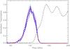 |
Fig. 4 Individual detector (blue dashed lines) and averaged (red line) normalised Ti–Al spectral response (ΔSi/ max(ΔSi), where ΔSi is the response of the ith pixel). The dispersion level between pixels is of the order of a few per cent. For illustration, the spectral response of the Ti–Al array is compared to the one of a pure 18 nm thick Al LEKID array with a Tc of approximately 1.4 K (dashed black line). |
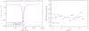 |
Fig. 5 Left: resonant frequency shift that si due to the variation of the SS temperature from 80 K to 300 K. Right: individual pixel sensitivities (blue diamonds) measured during tests compared to the reference goal (dashed red line). |
4.2. Spectral transmission
The gap of the Ti–Al bi-layer was measured from the absorption spectra taken in the laboratory using the MPI. The results are shown in Fig. 4. We observe that below about 65 GHz, a very low level of radiation is transmitted (lower than 5%). This means that the resulting energy gap for the Ti–Al films is ≈135 μeV, in agreement with the critical temperature. The corresponding spectrum bandwidth6Δν/ν was measured to be equal to 0.28.
4.3. Optical response and noise-equivalent power
The optical responsivity of the pixels was measured using the VNA. We performed frequency sweeps to measure the LEKID transfer function for various SS background temperatures. In Fig. 5 we present the shift of the resonant frequency for one pixel when the SS temperature is changed from 80 to 300 K. This frequency shift averaged across all the pixels corresponds to about 27 kHz. Using the optical model, we estimate the corresponding variation in optical power per pixel to be about 0.3 pW. This means that the averaged responsivity for the array is ℜ = 90 kHz/pW.
The spectral noise density Sn(f) (in Hz/) was calculated at a fixed SS temperature of 80 K using the NIKEL electronics. Correlated electronic noise was removed by subtracting a common mode. This was obtained by averaging the time-ordered-data (TOD) of all detectors in the array. The resulting template was fitted linearly to the TOD of each detectors. The best-fit was then subtracted from the detector TODs. After de-correlation, the spectral noise density is flat in a band between 1 and 10 Hz and equal to about Sn(f) = 1–3 Hz/. We can easily compute the NEP as
 The right panel of Fig. 5 shows the NEP of individual pixels. The best pixel has a NEP equal to 1.4 × 10⁻¹⁷ W/Hz0.5. The averaged NEP over all the array is 2.2 × 10⁻¹⁷ W/Hz0.5, which is about twice the goal.
5. Conclusion
We have produced and tested high-quality LEKID detectors based on multi-layer superconductor films. They have proved to be sensitive in the frequency range from 80 to 120 GHz.
We achieved internal quality factors exceeding 5 × 10⁴ under a typical space-like optical background of 0.4 pW, and we controlled the transition temperature as expected from calculations.
The spectral response agrees with the design. It peaks at 100 GHz with a 28% bandwidth.
The noise-equivalent power is very uniform across the array; the best pixels approach the reference NEP goal. On average, the NEP is about twice that of the goal.
We note that the LEKID design adopted for this study was originally developed for thin (thinner than 20 nm) Al films and ground-based typical optical backgrounds. The sensitivity could therefore be further improved by optimising, for example, the films, back-short, and substrate thicknesses, the resonator coupling to the RF feed-line and the meander geometry. Building on these promising results, larger arrays (hundreds of pixels) will be developed to investigate and mitigate, as we did already for Al films, systematic effects such as crosstalk between pixels and homogeneity over the array.
In this paper we call standard superconductors those that follow the superconductivity theory proposed by John Bardeen, Leon Cooper, and John Robert Schrieffer (BCS).
For an NIKA Al LEKID, the contribution of the detector noise has been measured to be lower than the other sources of noise and relatively flat in frequency.
The throughput is the name of the optical invariant that is used for the product of the pupil area and the solid angle subtended at this pupil.
The bandwidth is defined as  , where the FWHM is the full width at half maximum of the spectrum and ν0 is the central frequency.
Acknowledgments
The engineers more involved in the experimental setup development are Gregory Garde, Henri Rodenas, Jean-Paul Leggeri, Maurice Grollier, Guillaume Bres, Christophe Vescovi, Jean-Pierre Scordilis, and Eric Perbet. We acknowledge more in general the crucial contributions of the whole Cryogenics and Electronics groups at Institut Néel and LPSC. The arrays described in this paper have been produced at the CEA Saclay and PTA Grenoble microfabrication facilities. This work has been supported as part of a collaborative project, SPACEKIDS, funded via grant 313320 provided by the European Commission under Theme SPA.2012.2.2-01 of Framework Programme 7.
References
- Adam, R., Comis, B., Macías-Pérez, J. F., et al. 2014, A&A, 569, A66 [NASA ADS] [CrossRef] [EDP Sciences] [Google Scholar]
- Bennett, C. L., Larson, D., Weiland, J. L., et al. 2013, ApJS, 208, 20 [Google Scholar]
- Bourrion, O., Vescovi, C., Bouly, J. L., et al. 2012, in SPIE Conf. Ser., 8452 [Google Scholar]
- Bueno, J., Coumou, P. C. J. J., Zheng, G., et al. 2014, Appl. Phys. Lett., 105, 192601 [NASA ADS] [CrossRef] [Google Scholar]
- Calvo, M., Roesch, M., Désert, F. X., et al. 2013, A&A, 551, L12 [NASA ADS] [CrossRef] [EDP Sciences] [Google Scholar]
- Calvo, M., D’Addabbo, A., Monfardini, A., et al. 2014, J. Low Temp. Phys., 176, 518 [NASA ADS] [Google Scholar]
- Catalano, A., Calvo, M., Ponthieu, N., et al. 2014, A&A, 569, A9 [NASA ADS] [CrossRef] [EDP Sciences] [Google Scholar]
- Cooper, L. N. 1961, Phys. Rev. Lett., 6, 689 [NASA ADS] [CrossRef] [Google Scholar]
- Day, P. K., LeDuc, H. G., Mazin, B. A., Vayonakis, A., & Zmuidzinas, J. 2003, Nature, 425, 817 [NASA ADS] [CrossRef] [PubMed] [Google Scholar]
- Doyle, S. 2008, Ph.D. Thesis, 1, 193 [Google Scholar]
- Doyle, S., Naylon, J., Mauskopf, P., Porch, A., & Dunscombe, C. 2007, in Eighteenth International Symposium on Space Terahertz Technology, ed. A. Karpov, 170 [Google Scholar]
- Doyle, S., Naylon, J., Mauskopf, P., et al. 2008, in SPIE Conf. Ser., 7020, 0 [Google Scholar]
- Fauvet, L., Macías-Pérez, J. F., Aumont, J., et al. 2011, A&A, 526, A145 [NASA ADS] [CrossRef] [EDP Sciences] [Google Scholar]
- Fauvet, L., Macías-Pérez, J. F., & Désert, F. X. 2012, Astropart. Phys., 36, 57 [NASA ADS] [CrossRef] [Google Scholar]
- Hu, W., & White, M. 1997, New A, 2, 323 [Google Scholar]
- Irwin, K. D., & Hilton, G. C. 2005, in Cryogenic Particle Detection, Topics in Applied Physics No. 99, ed. C. Enss (Berlin Heidelberg: Springer), 63 [Google Scholar]
- Kogut, A., Banday, A. J., Bennett, C. L., et al. 1996, ApJ, 470, 653 [NASA ADS] [CrossRef] [Google Scholar]
- Kogut, A., Fixsen, D. J., Chuss, D. T., et al. 2011, J. Cosmol. Astropart. Phys., 7, 25 [Google Scholar]
- Leduc, H. G., Bumble, B., Day, P. K., et al. 2010, Appl. Phys. Lett., 97, 102509 [NASA ADS] [CrossRef] [Google Scholar]
- Martinis, J. M., Hilton, G. C., Irwin, K. D., & Wollman, D. A. 2000, Nucl. Instrum. Meth. Phys. Res. A, 444, 23 [NASA ADS] [CrossRef] [Google Scholar]
- Matsumura, T., Akiba, Y., Borrill, J., et al. 2014, J. Low Temp. Phys., 176, 733 [NASA ADS] [CrossRef] [Google Scholar]
- Mennella, A., Bersanelli, M., Butler, R. C., et al. 2011, A&A, 536, A3 [NASA ADS] [CrossRef] [EDP Sciences] [Google Scholar]
- Monfardini, A., Benoit, A., Bideaud, A., et al. 2011, ApJS, 194, 24 [NASA ADS] [CrossRef] [Google Scholar]
- Nagel, U., Nowak, A., Gebauer, H.-J., et al. 1994, J. Appl. Phys., 76, 4262 [NASA ADS] [CrossRef] [Google Scholar]
- Planck Collaboration I. 2014, A&A, 571, A1 [NASA ADS] [CrossRef] [EDP Sciences] [Google Scholar]
- Planck Collaboration XVI. 2014, A&A, 571, A16 [NASA ADS] [CrossRef] [EDP Sciences] [Google Scholar]
- Plank Collaboration Int. XXIX. 2014, A&A, submitted [arXiv:1409.2495] [Google Scholar]
- Planck HFI Core Team 2011, A&A, 536, A4 [NASA ADS] [CrossRef] [EDP Sciences] [Google Scholar]
- Swenson, L. J., Day, P. K., Eom, B. H., et al. 2013, J. Appl. Phys., 113, 104501 [NASA ADS] [CrossRef] [Google Scholar]
- Usadel, K. D. 1970, Phys. Rev. Lett., 25, 570 [CrossRef] [Google Scholar]
- Zmuidzinas, J. 2012, Ann. Rev. Condensed Matter Phys., 3, 169 [Google Scholar]
All Tables
All Figures
|
Fig. 1 Single Ti–Al bi-layer LEKID resonator design (top). The resonator is composed of a long inductive meander line and a capacitive element that is also used for tuning the resonant frequency. The effective sheet impedance of the meander line (seen by GHz–THz photons) is adjusted by the geometrical filling factor for a given the film resistivity. To optimise 100 GHz photon absorption, the pixels are back-illuminated through the silicon substrate. In addition, we use a back-short cavity situated at an optimised distance of 750 μm from the pixels (bottom). |
| In the text | |
|
Fig. 2 Left: ray-tracing snapshot of the cold optics inside the cryostat. Right: optical background estimation as a function of 100 mK cold stop aperture diameter (red line). We compare this result to the optical background measured in the HFI 100 GHz channel (violet dashed line). |
| In the text | |
|
Fig. 3 Left: frequency sweep of the first generation of 25 pixels Al–Ti array. Right: internal quality factor distribution. |
| In the text | |
|
Fig. 4 Individual detector (blue dashed lines) and averaged (red line) normalised Ti–Al spectral response (ΔSi/ max(ΔSi), where ΔSi is the response of the ith pixel). The dispersion level between pixels is of the order of a few per cent. For illustration, the spectral response of the Ti–Al array is compared to the one of a pure 18 nm thick Al LEKID array with a Tc of approximately 1.4 K (dashed black line). |
| In the text | |
|
Fig. 5 Left: resonant frequency shift that si due to the variation of the SS temperature from 80 K to 300 K. Right: individual pixel sensitivities (blue diamonds) measured during tests compared to the reference goal (dashed red line). |
| In the text | |
Current usage metrics show cumulative count of Article Views (full-text article views including HTML views, PDF and ePub downloads, according to the available data) and Abstracts Views on Vision4Press platform.
Data correspond to usage on the plateform after 2015. The current usage metrics is available 48-96 hours after online publication and is updated daily on week days.
Initial download of the metrics may take a while.