| Issue |
A&A
Volume 583, November 2015
|
|
|---|---|---|
| Article Number | A97 | |
| Number of page(s) | 8 | |
| Section | Numerical methods and codes | |
| DOI | https://doi.org/10.1051/0004-6361/201526426 | |
| Published online | 02 November 2015 | |
Simulating charge transport to understand the spectral response of Swept Charge Devices
1 Manipal Centre for Natural Sciences (MCNS), Manipal University, Manipal, Karnataka 576104, India
e-mail: athray@gmail.com
2 Indian Institute of Astrophysics (IIA), 560034 Koramangala, Bangalore, India
3 ISRO Satellite Centre, 560017 Bangalore, India
4 Centre for Electronic Imaging, The Open University, Milton Keynes MK7 6AA, UK
Received: 28 April 2015
Accepted: 27 August 2015
Context. Swept Charge Devices (SCD) are novel X-ray detectors optimized for improved spectral performance without any demand for active cooling. The Chandrayaan-1 X-ray Spectrometer (C1XS) experiment onboard the Chandrayaan-1 spacecraft used an array of SCDs to map the global surface elemental abundances on the Moon using the X-ray fluorescence (XRF) technique. The successful demonstration of SCDs in C1XS spurred an enhanced version of the spectrometer on Chandrayaan-2 using the next-generation SCD sensors.
Aims. The objective of this paper is to demonstrate validation of a physical model developed to simulate X-ray photon interaction and charge transportation in a SCD. The model helps to understand and identify the origin of individual components that collectively contribute to the energy-dependent spectral response of the SCD. Furthermore, the model provides completeness to various calibration tasks, such as generating spectral matrices (RMFs – redistribution matrix files), estimating efficiency, optimizing event selection logic, and maximizing event recovery to improve photon-collection efficiency in SCDs.
Methods. Charge generation and transportation in the SCD at different layers related to channel stops, field zones, and field-free zones due to photon interaction were computed using standard drift and diffusion equations. Charge collected in the buried channel due to photon interaction in different volumes of the detector was computed by assuming a Gaussian radial profile of the charge cloud. The collected charge was processed further to simulate both diagonal clocking read-out, which is a novel design exclusive for SCDs, and event selection logic to construct the energy spectrum.
Results. We compare simulation results of the SCD CCD54 with measurements obtained during the ground calibration of C1XS and clearly demonstrate that our model reproduces all the major spectral features seen in calibration data. We also describe our understanding of interactions at different layers of SCD that contribute to the observed spectrum. Using simulation results, we identify the origin of different spectral features and quantify their contributions.
Key words: X-rays: general / instrumentation: detectors / methods: numerical
© ESO, 2015
1. Introduction
Swept Charge Devices (SCD) are one-dimensional X-ray CCDs developed by e2v technologies Ltd., UK, to achieve good spectral performances at elevated operating temperatures. An array of twenty-four SCDs (CCD54) with a geometric area of ~1 cm2 each was used in the Chandrayaan-1 X-ray Spectrometer (C1XS) experiment (Howe et al. 2009; Grande et al. 2009) onboard the Chandrayaan-1 spacecraft. Chandrayaan-1 was launched successfully on 28 October 2008 with eleven scientific experiments to study the Moon in multiwavelengths. C1XS had the opportunity to decipher the lunar surface chemistry by measuring the XRF signals of all major rock-forming elements, (Na), Mg, Al, Si, Ca, Ti, and Fe, which are excited by the solar X-rays on the Moon simultaneously.
C1XS is one of the well-calibrated X-ray instruments that studied the chemical composition of the lunar surface with a good spectral resolution (onboard resolution ~153 eV at 5.9 keV). C1XS observed the Moon under different solar flare conditions for a period of nine months from November 2008 to August 2009. C1XS observations were duly supported by the simultaneous measurement of incident solar X-ray spectrum by the X-ray Solar Monitor (XSM) onboard Chandrayaan-1. Along with detecting major rock-forming elements (Narendranath et al. 2011), C1XS was the first instrument to observe the direct spectral signature of the moderately volatile element Na (1.04 keV) (Athiray et al. 2014) from the lunar surface. These results opened up a new dimension in our current understanding of the lunar surface evolution and raised new questions about the inventory of volatiles on the Moon. Unfortunately C1XS could not complete its objective of global elemental mapping due to the lack of solar X-ray activity and limited mission life. The limited weak flare C1XS observations resulted in a coarse spatial elemental mapping of certain regions of the Moon. The upcoming Chandrayaan-2 Large Area Soft X-ray Spectrometer (CLASS) experiment is being developed to continue and complete the global mapping of lunar surface chemistry. CLASS will use the second generation of SCDs (CCD236), which benefit from increased detector area and modified device architecture for improved radiation hardness (Gow et al. 2012).
X-ray detectors with good sensitivity and spectral resolution are needed to spectrally resolve the closely spaced lunar XRF lines Na (1.04 keV), Mg (1.25 keV), Al (1.48 keV), and Si (1.75 keV). The measured XRF line fluxes should have minimal uncertainties because the errors in the derived elemental abundances are directly coupled to XRF line flux errors (Athiray et al. 2013). Thus the accuracy of results depends on a good understanding of the instrument and the construction of a realistic detector spectral response from calibration data. A physical model incorporating the physics of charge generation and transportation in a device whose architecture is known provides complementarity and completeness to the measured calibration data, while also enabling the tuning of the device operation and event-selection criteria to optimize performance. In this paper, we present the charge transport model developed to simulate the spectral response of the SCD.
In Sect. 2 we describe the architecture of the SCD CCD54 used in C1XS and explain its clocking and read-out mechanism along with the different event selection processes adopted in the C1XS experiment. The algorithm developed to model charge transport, a description of charge transport model with fundamental assumptions, necessary equations, and its implementation are all explained in detail in Sect. 3. A brief summary of the C1XS ground calibration is presented in Sect. 4, which are used for the validation of charge transport model. Salient features of the simulation, results, and comparison with C1XS ground calibration data are presented in Sect. 5, and the conclusions inferred from this model are summarized in Sect. 6.
2. Swept Charge Devices used in C1XS
SCDs are modified versions of conventional X-ray CCDs specially designed for non-imaging, spectroscopic studies. The C1XS experiment used an array of 24 SCDs (Lowe et al. 2001) to record X-ray emission in the energy range of 0.8 to 20 keV. It offers good spectral resolution at benign operating temperatures, allowing the C1XS detectors to be operated between –10°C to +5°C using a passively cooled system. The SCD CCD54 has an active area of 1.07 cm2 per SCD and contains 1725 diagonal silicon electrodes with channel stops arranged in a herringbone structure, and the structure is shown in Fig. 1a. The device has an n-type buried channel beneath the electrodes where charges generated by photon or particle interactions are collected. The pitch of the channel stop is 25 μm (Gow 2009) and require 575 clock triplets to completely flush the SCD.
2.1. Clocking and read-out in SCD
The SCD operation is similar to a conventional X-ray CCDs where clock voltages are applied to electrodes to transfer charges collected in the buried channel. The difference is due to the novel electrode architecture implemented in the SCD, shown in Fig. 1a, which enables a large detector area to be read out quickly. SCDs are operated in continuous clocking mode at high frequencies (~100 kHz; Gow 2009), the continuously clocking suppresses the surface component of dark current and allows for operation at warmer temperatures when compared to a conventional 2D X-ray CCD. The term “pixel”, which refers to photon interaction co-ordinates on the device in conventional CCD, is not strictly applicable for a SCD. We refer to the photon interaction region on a device as elements, which are shown in Fig. 1b. These elements in each electrode are analogous to pixels in a 2D X-ray CCD. Charges collected within each element under different electrodes are clocked toward the central diagonal channel and then clocked down to reach the readout node (arrows in Fig. 1a indicate direction of charge flow). Charges collected in each electrode are subject to the same number of clock cycles to reach the readout node where they are merged to give a pseudo linear output. We refer to the combination of charges from these elements at the readout node assamples. The result of this method of operation is that the linear readout does not immediately provide information about where the photons were incident. Various advantages of SCD over conventional X-ray CCDs are given in Gow (2009).
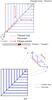 |
Fig. 1 a) Schematic view of the SCD CCD54; b) representation of elements in a diagonal electrode of SCD CCD54. Regions in the zoomed electrode are the elements which are separated by channel stops. |
2.2. Event processing in SCD
To control data volume, two event-processing modes were adopted in C1XS: time-tagged mode (during low and moderate event rates) and spectral mode (high event rate; Howe et al. 2009). Because the observed C1XS event rate was low throughout the mission, events were processed in time-tagged mode where each event was attached with onboard time and SCD number. This mode was further subdivided into two other modes based on event rates and a two-threshold logic:
-
1.
Multi-pixel mode (≤51 events/s – Type 11 data): out of a group ofthree adjacent pixels, if central pixel is above threshold 1, thenstore all the three events.
-
2.
Single-pixel mode (51−129 events/s – Type 10 data): out of a group of three adjacent pixels, only the central pixel event is stored if it is above threshold 1, and both the adjacent pixels are below threshold 2. Otherwise discard the central event.
Pictorial representation of single-pixel mode is shown in Fig. 2, thus the distribution of charges collected due to a photon event varies with different selection modes. This leads to different spectral shapes and in turn has an effect on the overall throughput of the detector.
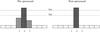 |
Fig. 2 Representation of “Single pixel (Type 10 data)” event selection logic used in C1XS with two threshold values Th1, Th2. |
2.3. Spectral redistribution function (SRF) of SCD
The interaction of X-ray photons within a detector results in a complex cascade of energy transfers with the energy deposited by each photon gets transformed in many ways, leading to various signatures in the observed energy spectrum. The distribution of all energy deposits above a noise threshold observed in a device by mono-energetic photons is called the spectral redistribution function (SRF).
In a SCD, charges collected from photon interaction are clocked diagonally and read out as a linear array of charges that are further processed for event recognition to obtain the spectrum. The observed SRF in SCD is thus a function of energy of the incident photon, the event selection logic, and threshold values. This model can be used to optimize threshold values used to select or reject split events. It can also identify the genesis of different features seen in the observed SRF and enables quantification of different process components.
3. Computation of SRF of SCD
In this section we describe the Monte Carlo algorithm used to simulate X-ray photon interactions and charge propagation in the SCD. A flowchart explaining the steps involved in the model is shown in Fig. 3. Fundamental assumptions of the model are listed below:
-
Si-based X-ray detector is assumed to be ideal, free of interstitialdefects and impurities.
-
The electric field is assumed to only be present perpendicular to the plane of the detector.
-
The acceptor impurity concentration in the field-free zone is assumed to be same as in the field zone.
-
The boundary between field and field-free zone is modeled with a small offset to avoid numerical divergence (at z0 = dd refer Eq. (5)).
These assumptions are related to the fabrication of X-ray devices for which direct experimental measurements are difficult to obtain, so major deviations in these assumptions will affect the detectors’ spectral performance. The epitaxial resistivity only decreases around a few μm near to the field-free zone and substrate boundary interface, which is difficult to measure. Large gradient in epitaxial resistivity amounts to charge losses via recombination. Si with large imperfections and defects will contribute to enhanced dark noise resulting in spectral degradation. However, no such effects were experienced in the ground calibration tests, as well as in flight observations; as a result, these assumptions are considered to be valid.
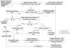 |
Fig. 3 Flowchart of the charge transport model to simulate the SRF of the SCD. Some of the important steps involved in the model are arranged in sequence. It is clear that the dead layer and substrate are included to account for photon loss while no charge is collected from the interaction. |
The vertical structure of the SCD discussed in this paper is shown in Fig. 4 with different layers labeled with respective dimensions. The dead layer ~1.5 μm thick, consists of SiO2, Si3N4, and poly silicon layer. A negligible fraction of X-ray photons interact in the dead layer and result in charge collection. We therefore modeled it as a single block of SiO2 from which no charge is collected. The bulk substrate is a heavily doped p+ region, where charges suffer huge losses owing to recombination, hence are considered to be lost.
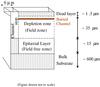 |
Fig. 4 Vertical structure of the SCD CCD54. Photon interaction in field zone, field-free zone, and channel stops contribute chiefly to the observed SRF. Interaction in bulk substrate and regions in dead layer and above result in a negligible amount of final charge collection. |
3.1. Photon interaction
Mono-energetic X-ray photons are simulated to illuminate the SCD at random positions (x, y) with uniform probability, at normal incidence angle with respect to the plane of SCD. These photons travel through different layers of the detector before interaction. The distribution of depths at which interactions occur inside the SCD is computed using 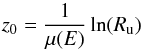 (1)where the μ(E) – linear mass absorption coefficient of the material at photon energy E, Ru – random number with uniform distribution. If the interaction depth (z0) is greater than the thickness of a layer, then the interaction depth is computed again, including the material in the following layer. Soft X-ray photons interact via the photoelectric process, resulting in a charge cloud (e-h pairs), which is assumed to be spherical in shape. The radial charge distribution of this spherical cloud is assumed to follow a Gaussian distribution with the 1σ radius given by Kurniawan & Ong (2007)
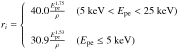 (2)where ρ – density of the detector material (ρ = 1.86 g/cc for Si), Epe – energy of the photo-electron. This implies that charges are concentrated toward the center of the sphere, fall off with radius, and abruptly truncate to zero at the cloud boundary. While estimating the number of charges produced by absorption of X-ray photon, Fano noise (Fano 1947; Owens et al. 2002) is important, which is incorporated as
 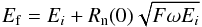 (3)where Ef – energy distribution with Fano noise added, Rn(0) – normally distributed random number with mean 0 and variance 1, F – Fano factor (F = 0.12 for Si) and ω – average energy required to produce an e-h pair (ω = 3.65 eV at 240 K for Si). The initial charge (Q0) is obtained from this final energy distribution (Ef) as
  (4)The interaction of X-ray photons in SCDs can be grouped into three regions based on the photon interaction zone: field zone, field-free zone, and channel stop. The escape peak appears as a consequence of X-ray photon interaction within the detector that also needs to be incorporated.
3.2. Field zone interactions
Photons interacting at depths within the depletion zone (i.e., z0<dd) are called field zone interactions. The thickness of the field zone mainly depends on the bias voltage and doping concentration. In the case of the SCD CCD54, with an acceptor impurity concentration (Na) of 4 × 10¹² atoms/cm3 and average depletion voltage of 9 V (Gow (2009), the depletion depth was found to be ~35 μm. The charge cloud produced here by a photon interaction will experience the complete electric field and will drift toward the buried channel. The radius of the charge cloud collected within the buried channel after charge spreading due to random thermal motions is given by (Hopkinson 1987) 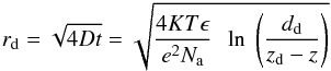 (5)where K is the Boltzmann constant, T the temperature in kelvin, e the electronic charge, ϵ the permitivity of Si, Na the doping concentration in Si, and dd the thickness of depletion depth.
3.3. Field-free zone interactions
In epitaxial devices, there is a field-free region between the field zone and the bulk Si substrate (p+) layer, which does not have an electric field (see Fig. 4) and exhibits a gradient in doping concentration near to the substrate boundary. Photon interactions in this region dd<z0<dd + zff are considered to be field-free zone interactions. Charge clouds produced within this region will not experience any acceleration but could diffuse and recombine before reaching the buried channel. Diffusion enlarges the size of the charge cloud and could cause spreading of charges across several adjacent elements. It is reasonable to assume that the recombination losses are negligible in this region due to large carrier lifetime (~10-3 s; Tyagi & van Overstraeten 1983). The general expression for the mean-square radius of charge cloud reaching the interface between the field and field-free zone is given by (Pavlov & Nousek 1999) ![\begin{equation} r_{\rm ff} = \sqrt{2d_{\rm ff}L~\biggl[\tan h\left(\frac{d_{\rm ff}}{L}\right) - \left(1-\frac{z-d_{\rm d}}{d_{\rm ff}}\right) \tan h\biggl(\frac{d_{\rm ff}-z+d_{\rm d}}{L}\biggr)\biggr]} \end{equation}](/articles/aa/full_html/2015/11/aa26426-15/aa26426-15-eq41.png) (6)where dff is the thickness of epitaxial field-free zone, L = diffusion length (
(6)where dff is the thickness of epitaxial field-free zone, L = diffusion length ( , τn is the charge carrier lifetime, and D the diffusion constant). It is evident from the above equation that when a photon interacts deeper in the field-free zone, the term (dff−z0 + dd) becomes very very small, so the radius (rff) becomes very large. It should be noted that the shape of the charge cloud in the field-free zone is non-Gaussian as investigated by Pavlov & Nousek (1999). However, here we assume that they are Gaussian because it only affects a few high energy photon events in the field-free zone. Thus, the final radius of the charge cloud is obtained as the quadrature sum of ri, rd, rff:
  (7)
(7)
3.4. Channel stop interactions
The channel stops occupy a considerable amount of area in the CCD54 (~20%), and photon interaction in channel stops can distort the shape of the observed SRF because it causes horizontal split events. We adopted the same approach followed in simulating the response of the CCDs in the Chandra Advanced CCD Imaging Spectrometer (ACIS; Townsley et al. 2002), where photons interacting in the channel stops (p+layer) are assumed to split the resulting charge and are collected on the left- and the righthand sides of the channel stop. The fraction of charges swept toward each side depends on the distance of each side from the location of interaction. Charges propagated from both the edges of a channel stop are found using (Townsley et al. 2002)  (8)where wc is the width of channel stop, χ the channel stop tuning loss parameter, and α the channel stop tuning width parameter. The interaction in within the channel stop region is complex because it involves interaction in the p+layer or directly underneath. It is shown from the detailed ACIS calibration (Townsley et al. 2002) that the channel-stop tuning parameters χ and α vary with incident photon energy, which require precise experimental data on channel stop interactions. However, for simplicity, we assume energy independence of these parameters in this work. From Eq. (8) it is clear that a change in χ and α with photon energy will modify the fraction of charges collected on either side of the channel stop and is expected to affect the distribution of horizontally split events, and this contributes to the non-photopeak events of the SRF.
3.5. Charge collection and read-out
The amount of charge collected in each element (i, j) at the gates is obtained by integrating the Gaussian function, which is given by Pavlov & Nousek (1999): ![\begin{eqnarray} Q_{ij}(x_0,y_0) &=& {\int}_{a_{i}}^{a_{i+1}}{\int}_{b_{i}}^{b_{i+1}} q({\vec{r}})~{\rm d}x{\rm d}y \nonumber\\ \label{eq:chargecollected} Q_{ij}(x_0,y_0) &=& \frac{Q_o}{4} \biggl\{\biggl[\mbox{erf}\biggl\{\frac{a_{i+1}-x_0}{r}\biggr) - \mbox{erf}\biggl(\frac{a_i-x_0}{r}\biggr)\biggr] \nonumber\\ & &\quad \times \biggl[\mbox{erf}\biggl(\frac{b_{i+1}-y_0}{r}\biggr) - \mbox{erf}\biggl(\frac{b_i-y_0}{r}\biggr)\biggr]\biggr\} \end{eqnarray}](/articles/aa/full_html/2015/11/aa26426-15/aa26426-15-eq58.png) (9)where r will be replaced with Eq. (7) for interaction in the field zone and field-free zone, respectively; a, b are pixel dimensions; x0 and y0 are the relative event coordinates in the reference frame with its origin at the center of the pixel where the photon is absorbed (–a/ 2 <x0<a/ 2, –b/ 2 <y0<b/ 2).
(9)where r will be replaced with Eq. (7) for interaction in the field zone and field-free zone, respectively; a, b are pixel dimensions; x0 and y0 are the relative event coordinates in the reference frame with its origin at the center of the pixel where the photon is absorbed (–a/ 2 <x0<a/ 2, –b/ 2 <y0<b/ 2).
In Sect. 2, we have indicated that the fundamental difference between the SCD and 2D CCD, primarily lie in the diagonal clocking and read-out. In our simulation, we modeled the elements as 2D pixels of equivalent dimensions. Charges collected in each of these equivalent pixels are computed using Eq. (9). Moreover, we incorporated the read-out structure by adding the charges collected at different elements of each electrode in the SCD.
3.6. Escape peak computation
Photons with incident energy Eph> 1.84 keV (i.e., binding energy of Si K-atomic shell electrons) have a finite probability of yielding Si K-α XRF photons of energy 1.74 keV. These XRF photons travel some distance before getting absorbed in the detector. XRF photons emitted from the top few microns of the detector have a high probability of escaping without being detected. In such cases, the residual charges were collected to form the escape peak with energy Eesc = E−1.84 keV. To simulate the escape peak, we find the number of Si XRF photons produced from a thick Si medium, where the photons are emitted in all possible directions. Directions are assigned using the uniform random number, in which half of the photons exiting the surface of the detector are considered to yield the escape peak feature.
3.7. Implementation
The algorithm explained in Fig. 3 is implemented with a set of IDL routines. Device level parameters, such as channel stop pitch, width, and acceptor impurities (NA) associated with the fabrication of SCD CCD54 provided by the manufacturer, are documented in Gow (2009). A thorough characterization and optimization of voltages carried out for the flight units of SCD CCD54 to achieve the expected spectral performance are summarized in Gow (2009). Values of some of the important detector parameters used in the model are listed in Table 1. A short summary of the implementation, highlighting the important steps are given below:
-
Allow photons to impinge on the SCD randomly at normalincidence (i.e., 0° with respect to detector normal) and obtain subpixel position coordinates (X, Y).
-
Separately tag photons interacting in channel stops and pixel regions.
-
Simulate physics of photon interaction and charge propagation separately in field zone, field-free zone, and channel stops.
-
Clock charges collected in the elements of SCD diagonally, then combine and read out as a linear array output.
-
Apply single-pixel mode event-selection logic with two threshold values.
-
Make histogram of the event processed output.
Values of parameters used in modeling charge transport of SCD.
4. Ground calibration of the SCD in C1XS – an overview
An extensive ground calibration was carried out for all the detectors in C1XS, using a double crystal monochromator in the RESIK X-ray beam-line at Rutherford Appleton Laboratory (RAL), UK. Distinct mono-energies were chosen for SRF measurements using the following target anodes: Ti (4.51 keV), Cr (5.414 keV), Co (6.93 keV), and Cu (8.04 keV). The mono-energetic beam was collimated using a rectangular slit of 1mm × 2mm dimension illuminating only a small portion of the SCD. Temperature dependence of the SRF parameters was also studied across a range from –30°C to –10°C. These calibration data were further processed for event recognition using a two-threshold logic explained in Sect. 2.2. Prominent spectral features seen in the filtered calibration data are photopeak, low energy shoulder, low energy tail, cut off, escape peak, and low energy rise. These spectral features were modeled empirically and interpolated throughout the entire energy range to create spectral response matrix of the SCD. It was also noted that the SRF components exhibit an energy dependence. Further details on the ground calibration of C1XS instrument can be found in Narendranath et al. (2010).
5. Simulation results – SRF components
Here we summarize our understanding of different spectral components that are seen in the observed SRF. From our simulation, we identified the sources of origin for the SRF components, which are summarized in Table 2.
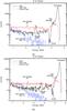 |
Fig. 5 Simulation results showing different components of SRF for different mono-energetic photons arising from interactions at different layers of SCD: a) 4.510 keV, b) 5.414 keV. |
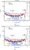 |
Fig. 6 Simulation results showing different components of SRF for different mono-energetic photons arising from interactions at different layers of SCD: a) 6.93 keV, b) 8.047 keV. |
5.1. SRF components – field zone
The dominant photopeak in the SRF mainly arise from field zone interactions, where charges are collected almost completely. Interactions that occur at element boundaries and at greater depths near to the boundary of field-free zone cause charge splitting across many elements. These charges are clocked diagonally and added appropriately to produce the soft-shoulder and low-energy tail. Si XRF photons emitted from the top layer of the field zone have a high probability of escaping and hence contributing to the escape peak. The simulated SRF due to field zone interactions for different X-ray energies are shown in Figs. 5a, b, 6a and b.
Cutoff is observed at two places in the energy spectrum, which are related to the value of threshold 1 (Th1):
-
Low energy cutoff : Events below threshold 1; i.e.,0.75 keV are discarded.
-
Soft shoulder cutoff: Charges that are split at pixel boundaries lead to configurations with central event discarded (see Fig. 2) causing a dip near the soft shoulder. The energy at which dip occurs in the spectrum depend on threshold 1 given by Edip ≈ Eph−Eth1.
5.2. SRF components – field-free zone
The charge cloud produced due to field-free zone interactions undergoes diffusion, causing charge to spill over multiple elements. As a result, a low-energy rising-tail component without a photopeak is observed in the pulse height distribution as shown in Figs. 5a, b, 6a, and b. This component is negligible for low energy X-ray photons as a majority of photons get absorbed above the field-free zone.
Identification of SRF components and its origin in the SCD – simulation results.
5.3. SRF components – channel stop
Channel stop interactions contribute partly to the soft shoulder component (near the photopeak) and also to the low-energy tail in the SRF as shown in Figs. 5a, b, 6a, and b.
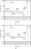 |
Fig. 7 Comparison of simulated SRF and the observed SRF from C1XS ground calibration: a) 4.510 keV, b) 5.414 keV. The bottom panel shows the difference between two SRFs. |
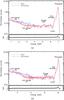 |
Fig. 8 Comparison of simulated SRF and the observed SRF from C1XS ground calibration: a) 6.93 keV b) 8.047 keV. The bottom panel shows the difference between two SRFs. |
5.4. Comparison of SRF simulation vs. SRF data
We demonstrate the performance of the model by comparing the simulated SRF with the SRF derived from C1XS ground calibration. It is clear that all the observed features arise from interactions at different layers of the detector, coupled with the threshold values and event selection logic. An overplot of simulation and calibration data that are normalized to total events for different energies is shown in Figs. 7a, b, 8a and b.
5.5. Statistical tests
To establish the robustness of the algorithm, the following standard statistical tests are performed on the data sets: SRF derived from simulation and calibration at different energies. A simple Student’s T-test is performed to verify the null hypothesis that the simulation and calibration data exhibit same means which are drawn from a population with same variance. The computed T-statistic values and significance are given in Table 3. The very low T-statistic values with high significance clearly show that the SRF of model and calibration have same mean values.
Simulated SRF vs. observed SRF – statistical tests results.
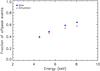 |
Fig. 9 Comparison of fraction of off-peak events as a function of photon energy between simulation (triangles) and calibration data (filled circles). |
A chi-square (χ2) test is often used to determine whether two binned data sets belong to the same parent distribution. It computes the differences between the binned data sets. The chi-square statistic computed for our data sets, the number of degrees of freedom (ν), and the corresponding chi-square probability are given in Table 3. A low χ2 value with high degrees of freedom (ν) yields a high probability that clearly indicates that the SRF derived from model and calibration data agree very closely.
Our simulation results predict all the major features seen in the experimentally derived SRF. The difference between data and model are represented as residuals in the bottom panel of each figure (Figs. 7a−8b). High energy X-ray photons penetrate deep inside the detector before interaction, hence additional interactions in the field-free zone causing more split events. The expected trend toward decreases in the photopeak and increases in off-peak events with increased X-ray energy is clearly seen. The variation in the fraction of off-peak events at different energies obtained from calibration data and simulation are plotted in Fig. 9, and a close match between the two clearly shows that the model represents the calibration data fairly well. It is noted that deviations are observed in predicting soft shoulder and low-energy tail components at higher X-ray energies. We attribute this discrepancy to incomplete modeling of the energy dependence in the channel stop interactions.
6. Conclusion
To conclude, we have successfully demonstrated the capability of our charge transport model in simulating the SRF of epitaxial
SCDs used in C1XS. Comparing the simulation results to the available ground calibration data clearly demonstrates that the SRF can be determined at different energies. The validation of simulation results with C1XS ground calibration data have provided physical reasoning for all the observed spectral features and also its energy dependence. Simulation results show a systematic underestimation of the fraction of offpeak events with an increase in photon energy. This discrepancy can be mitigated by including the energy dependence of channel-stop tuning parameters, and this would require further detailed experiments. Also the interaction within the dead layer and substrate are considered to be lost, which would need to be included for very low energy and high energy X-ray photons.
References
- Athiray, P. S., Sudhakar, M., Tiwari, M. K., et al. 2013, Planet. Space Sci., 89, 183 [NASA ADS] [CrossRef] [Google Scholar]
- Athiray, P. S., Narendranath, S., Sreekumar, P., & Grande, M. 2014, Planet. Space Sci., 104, 279 [NASA ADS] [CrossRef] [Google Scholar]
- Fano, U. 1947, Phys. Rev., 72, 26 [NASA ADS] [CrossRef] [Google Scholar]
- Gow, J. 2009, Ph.D. Thesis, Brunel Univ., UK [Google Scholar]
- Gow, J. P. D., Holland, A. D., Pool, P. J., & Smith, D. R. 2012, Nucl. Instr. Meth. Phys. Res. A, 680, 86 [NASA ADS] [CrossRef] [Google Scholar]
- Grande, M., Maddison, B. J., Howe, C. J., et al. 2009, Planet. Space Sci., 57, 717 [NASA ADS] [CrossRef] [Google Scholar]
- Hopkinson, G. R. 1987, Opt. Engin., 26, 766 [NASA ADS] [Google Scholar]
- Howe, C. J., Drummond, D., Edeson, R., et al. 2009, Planet. Space Sci., 57, 735 [NASA ADS] [CrossRef] [Google Scholar]
- Kurniawan, O., & Ong, V. K. S. 2007, Scanning, 29, 280 [CrossRef] [Google Scholar]
- Lowe, B. G., Holland, A. D., Hutchinson, I. B., Burt, D. J., & Pool, P. J. 2001, Nucl. Instr. Meth. Phys. Res. A, 458, 568 [NASA ADS] [CrossRef] [Google Scholar]
- Narendranath, S. 2011, Ph.D. Thesis, Univ., of Calicut, Kerala, India [Google Scholar]
- Narendranath, S., Sreekumar, P., Maddison, B. J., et al. 2010, Nucl. Instr. Meth. Phys. Res. A, 621, 344 [NASA ADS] [CrossRef] [Google Scholar]
- Narendranath, S., Athiray, P. S., Sreekumar, P., et al. 2011, Icarus, 214, 53 [NASA ADS] [CrossRef] [Google Scholar]
- Owens, A., Fraser, G. W., & McCarthy, K. J. 2002, Nucl. Instr. Meth. Phys. Res. A, 491, 437 [NASA ADS] [CrossRef] [Google Scholar]
- Pavlov, G. G., & Nousek, J. A. 1999, Nucl. Instr. Meth. Phys. Res. A, 428, 348 [Google Scholar]
- Townsley, L. K., Broos, P. S., Chartas, G., et al. 2002, Nucl. Instr. Meth. Phys. Res. A, 486, 716 [NASA ADS] [CrossRef] [Google Scholar]
- Tyagi, M. S., & van Overstraeten, R. 1983, Solid State Electro., 26, 577 [NASA ADS] [CrossRef] [Google Scholar]
All Tables
All Figures
|
Fig. 1 a) Schematic view of the SCD CCD54; b) representation of elements in a diagonal electrode of SCD CCD54. Regions in the zoomed electrode are the elements which are separated by channel stops. |
| In the text | |
|
Fig. 2 Representation of “Single pixel (Type 10 data)” event selection logic used in C1XS with two threshold values Th1, Th2. |
| In the text | |
|
Fig. 3 Flowchart of the charge transport model to simulate the SRF of the SCD. Some of the important steps involved in the model are arranged in sequence. It is clear that the dead layer and substrate are included to account for photon loss while no charge is collected from the interaction. |
| In the text | |
|
Fig. 4 Vertical structure of the SCD CCD54. Photon interaction in field zone, field-free zone, and channel stops contribute chiefly to the observed SRF. Interaction in bulk substrate and regions in dead layer and above result in a negligible amount of final charge collection. |
| In the text | |
|
Fig. 5 Simulation results showing different components of SRF for different mono-energetic photons arising from interactions at different layers of SCD: a) 4.510 keV, b) 5.414 keV. |
| In the text | |
|
Fig. 6 Simulation results showing different components of SRF for different mono-energetic photons arising from interactions at different layers of SCD: a) 6.93 keV, b) 8.047 keV. |
| In the text | |
|
Fig. 7 Comparison of simulated SRF and the observed SRF from C1XS ground calibration: a) 4.510 keV, b) 5.414 keV. The bottom panel shows the difference between two SRFs. |
| In the text | |
|
Fig. 8 Comparison of simulated SRF and the observed SRF from C1XS ground calibration: a) 6.93 keV b) 8.047 keV. The bottom panel shows the difference between two SRFs. |
| In the text | |
|
Fig. 9 Comparison of fraction of off-peak events as a function of photon energy between simulation (triangles) and calibration data (filled circles). |
| In the text | |
Current usage metrics show cumulative count of Article Views (full-text article views including HTML views, PDF and ePub downloads, according to the available data) and Abstracts Views on Vision4Press platform.
Data correspond to usage on the plateform after 2015. The current usage metrics is available 48-96 hours after online publication and is updated daily on week days.
Initial download of the metrics may take a while.