Fig. 2
Download original image
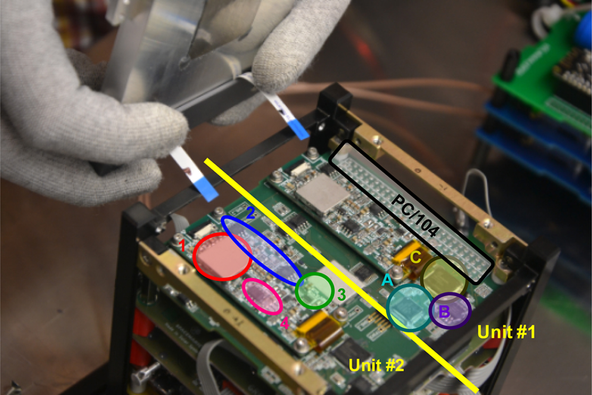
Payload components of the GRBAlpha nano satellite. The numbers indicate the daughterboard containing the analog and mixed-signal components for payload unit #2: 1 (red): adjustable high-voltage supply for MPPC reverse biasing, shielded; 2 (blue): Preamplifier and signal shaping circuitry; 3 (green): analog-digital converter; 4 (magenta): High-voltage control logic. The letters indicate the main PC/104 board with the digital control and signal processing parts for payload unit #1 : A (cyan): microcontroller unit; B (lilac): FPGA configuration FRAM, also used as a secondary staging area for firmware upgrades; C (yellow): FPGA responsible for the interface between the mixed-signal components on the daughterboard and the MCU. The PC/104 system bus connector can be seen at the top right of the figure. This photo was taken during the integration of the satellite when the scintillator block was attached electrically to the daughterboards using the white-blue flex cables.
Current usage metrics show cumulative count of Article Views (full-text article views including HTML views, PDF and ePub downloads, according to the available data) and Abstracts Views on Vision4Press platform.
Data correspond to usage on the plateform after 2015. The current usage metrics is available 48-96 hours after online publication and is updated daily on week days.
Initial download of the metrics may take a while.