Fig. 1
Download original image
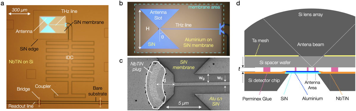
Detector geometry. (a) Micrograph of a single detector, consisting of a NbTiN CPW line loaded with an IDC coupled to the readout line via a coupling structure. Its shorted end consists of an aluminium section fabricated on a thin SiN membrane, which is highlighted by the backlighting in the micrograph. (b) Zoom onto the aluminium section on the SiN membrane with the leaky-slot antenna coupled to a co-planar waveguide line (referred to as THz line), where radiation absorption takes place. (c) Scanning electron microscope image of the antenna centre showing the THz line in detail and the NbTiN quasiparticle plug. The THz line dimensions are: wg = 1.2 µm and wc = 0.4 µm. (d) Cross-sectional diagram of the detector assembly (not to scale). The detector chip, as depicted in panels a-c, is coupled to a Si lens array using a spacer wafer with a Ta absorbing mesh, with an opening aligned to the antenna to enable radiation coupling. The vacuum gap t is created using spin-on PermiNex® glue pillars as indicated.
Current usage metrics show cumulative count of Article Views (full-text article views including HTML views, PDF and ePub downloads, according to the available data) and Abstracts Views on Vision4Press platform.
Data correspond to usage on the plateform after 2015. The current usage metrics is available 48-96 hours after online publication and is updated daily on week days.
Initial download of the metrics may take a while.