Fig. 2
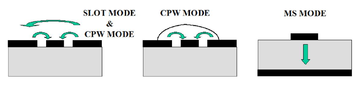
Schematic cut through a KID substrate. In grey, the high-resistance silicon wafer, while in black, the aluminium films are represented. The green arrows illustrate the direction of the electric field. Left: the co-planar waveguide (CPW) transmission line without across-the-line bondings, associated to strongly non-uniform performance of the detector array. Centre: CPW with across-the-line bondings, configuration adopted in NIKA. Right: the microstrip (MS) configuration adopted in NIKA2, ensuring single-mode propagation and easiest implementation of very large arrays.
Current usage metrics show cumulative count of Article Views (full-text article views including HTML views, PDF and ePub downloads, according to the available data) and Abstracts Views on Vision4Press platform.
Data correspond to usage on the plateform after 2015. The current usage metrics is available 48-96 hours after online publication and is updated daily on week days.
Initial download of the metrics may take a while.